EUV lithography machine heavy report, the United States released.
Editor's Note: Recently, the U.S. NIST has released a significant report on EUV lithography machines. In it, they summarize and look forward to the current status and future of EUV lithography development.
The following is the main body of the article:
Introduction
In 2022, the semiconductor market size was approximately 0.6 trillion U.S. dollars, and business analysts predict that it will double by 2030, reaching 1.0 to 1.3 trillion U.S. dollars. The substantial growth in the semiconductor manufacturing industry can be reflected in the lithography process. Lithography is a patterning process that transfers planar designs to the surface of a wafer substrate, forming complex structures such as transistors and wiring interconnections. This is accomplished through a complex multi-step process that selectively exposes photosensitive polymers or photoresists to light of a specific wavelength. Recently, the advancement of lithography technology has created a competitive edge in the production of the most advanced semiconductors, making the most advanced technologies such as artificial intelligence (AI), 5G communication, and supercomputing possible. Therefore, advanced semiconductor technology will greatly affect national security and economic prosperity.
The most advanced semiconductor lithography process in use today employs EUV light sources, particularly light at 13.5 nm. EUV light allows for the construction of smaller unit features in semiconductors. It is reported that the EUVL system currently costs 150 million U.S. dollars and was first deployed by ASML in 2019, a company that has maintained a 100% market share. To date, ASML has delivered three different models of EUVL systems, namely Twinscan NXE:3400 B/C and NXE:3600D, with the total shipment of NXE systems increasing from 31 units in the first quarter of 2019 to 181 units in the last quarter of 2022.
Advertisement
The organization of this report is as follows. The remainder of the introduction includes the technical background of EUVL, the background of the international and domestic status of EUVL, and an overview of the NIST and CHIPS R&D metrology program. Section 2 contains the status and needs of EUVL technology discussed at the working group meeting. Section 3 outlines the survey results and recommendations for the way forward from the working group meeting, concluding the report.
Technical Background of EUV Lithography
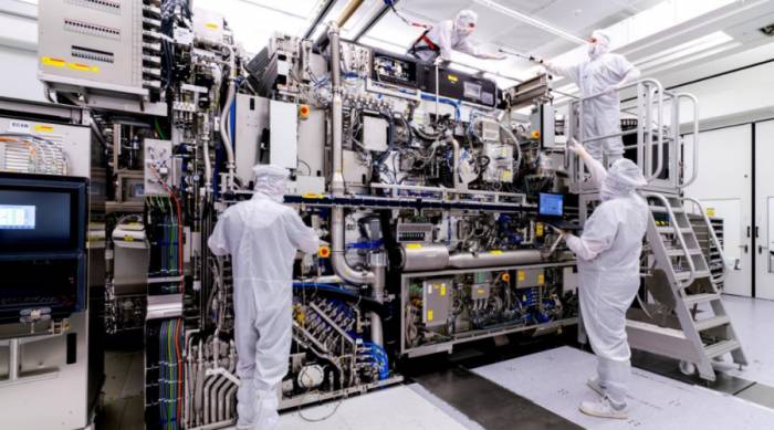
EUVL is a key step in manufacturing the next generation of semiconductor chips. EUV light is produced by high-temperature plasma generated by high-purity tin. Solid tin is melted inside a droplet generator, which continuously produces over 3 million 27-micron droplets per minute in a vacuum chamber. A carbon dioxide (CO2) laser with an average power of 25 kW irradiates the tin droplets with two consecutive pulses, shaping and ionizing the droplets. Initially, several kilowatts of EUV light were produced, but only a small portion of the light reaches the photomask due to absorption and scattering losses along the optical path. The output power and beam quality of 13.5 nm light are inferred from measurements of an indirect fluorescence camera. A multilayer condenser mirror system guides the light onto the photosensitive polymer or photoresist, transferring the pattern to the silicon wafer. The reflecting mirrors are protected from tin debris by a constant flow of H2 gas. The automatic wafer stage positions the wafer with a resolution of ≤0.25 nm after each exposure, with a 20,000-cycle inspection and adjustment process per second. Overall, this process requires precise coordination between many different engineering systems. Figure 1 shows a photo of the ASML-EUVL components.
Current Status and Future of EUV Lithography Technology
The growth of the advanced semiconductor manufacturing industry comes from new EUV manufacturing equipment in the United States, as well as Europe and Asia. As mentioned earlier, the only company currently producing EUVL scanner components is ASML, headquartered in the Netherlands. ASML sells EUV scanner components to companies such as Intel, TSMC (headquartered in Taiwan, China), and Samsung (headquartered in South Korea). These companies then use EUV scanners in their semiconductor manufacturing equipment. The EUVL system is not only manufactured in the Netherlands but consists of many modules developed globally, which are shipped to ASML's headquarters in the Netherlands for final assembly and testing before delivery to customers. Readers can refer to relevant literature reports for more details on the supply chain in the microelectronics manufacturing ecosystem.From the perspective of the United States, ASML's EUV light source research and development and manufacturing base is located in San Diego, California. The light source component of the EUVL scanner is shown in Figure 2. It should be noted that the light source component includes the source container located in the EUVL scanner component, as well as many other components, including laser metrology, beam transfer systems, and driver lasers and their auxiliary equipment. Cymer, based in San Diego, is responsible for the EUV light source-related work and was acquired by ASML in 2012. In addition, given the advantages of EUVL in semiconductor manufacturing, export controls protect this technology. Specifically, in October 2022, the U.S. Bureau of Industry and Security (BIS) issued a rule - 87 FR 62186, to control the export of technologies including extreme ultraviolet lithography.
ASML stated that the future development of EUV lithography includes increasing the numerical aperture (NA) from 0.33 to 0.55 ("High NA"). High NA can reduce the number of multiple patterning steps required by the current 0.33NA and can address finer geometric dimensions. This is consistent with the 2022 IEEE International Device and System Roadmap (IRDS) published publicly and is necessary to continue scaling the transistor to 0.5 nanometers by 2037. The new NA platform aims to improve the change rate of the wafer and mask state to achieve geometric chip scaling. The High NA system is expected to be delivered to customers in 2023, and the full platform process for mass production is expected to be operational in 2025. In early 2023, ASML announced that they set two new EUV power records, that is, the High NA lithography machine model EXE: 5200 running 600 W EUV for one hour meets the dose stability specifications and can perform open-loop operation at 700 W. Before the realization of EUV mass production, the 600 W demonstration has increased compared to the 250 W delivered five years ago. Sections 2.1 and 2.2 contain detailed information about the 600 W power demonstration of the droplet generator and laser power. Other details about High NA are not within the scope of this report. Nevertheless, readers can refer to a paper by Levinson in 2022 for more information on the current status and prospects of High NA EUVL.
Understanding the international and domestic situation of EUVL helps to understand R&D cooperation opportunities and emphasizes the competitive landscape of the technology field and the necessity of scientific leadership. Finally, given that the funding of the CHIPS Act is to improve the resilience of the U.S. semiconductor manufacturing industry, people must be aware of the importance of helping to produce this key manufacturing process through first-class measurement practices.
NIST and CHIPS R&D Measurement Program Overview
Dr. Marla Dowell, Director of the CHIPS R&D Measurement Program and NIST Boulder Laboratory, gave a welcome speech at the working group meeting. The keynote speech first reminded participants of NIST's mission:
By advancing measurement science, standards, and technology, to enhance economic security and improve our quality of life, and to promote innovation and industrial competitiveness in the United States.
It emphasized NIST's core capabilities: (1) measurement science, (2) rigorous traceability, and (3) the development and use of standards. Dr. Dowell provided more details about the chip R&D measurement program, organizational relationships, and the background of NIST's national research institutions. Dr. Dowell emphasized the necessity of joint research between the industry and NIST to cooperate in solving urgent microelectronics challenges that are crucial to chips. He reminded the audience that NIST is a non-regulatory laboratory. Therefore, NIST has always been a reliable partner for proprietary information, maintaining neutrality and objectivity, and promoting the development of key technologies by disseminating high-quality measurements, data, and research that support American innovation and industrial competitiveness. Specifically, in Boulder, NIST has about 900 employees and more than 500,000 square feet of laboratory space, covering six areas, including (1) advanced communication technology, (2) quantum science and engineering, (3) time and frequency metrology, (4) advanced material characterization, (5) precision imaging, (6) lasers and optoelectronics. Dr. Dowell then emphasized that NIST has a long history and a broad target investment portfolio in the field of microelectronics, covering many areas.
Dr. Dowell later turned to speak about the American CHIPS Act. An outline of the strategy of the U.S. chip fund was given, including how it will support three different initiatives: (1) large-scale investment in cutting-edge manufacturing; (2) new manufacturing capabilities for mature and current generation chips, new technologies, and professional techniques, as well as semiconductor industry suppliers; (3) initiatives to strengthen the U.S. R&D leadership position. The distinction was made between the $39 billion in manufacturing incentives and the $11 billion in R&D incentives, focusing on the allocation of R&D funds and the NIST measurement science section. Dr. Dowell discussed how to seek extensive feedback from industry, academia, and government stakeholders in various forms through seven identified strategic opportunities for the U.S. semiconductor manufacturing industry, including activities such as EUVL working group meetings.The Communication Technology Laboratory (CTL) provided an example of metrology in materials measurement. Before becoming the director of the chip development metrology project, she served as the head of the operations department, mainly responsible for the standard reference materials (SRM) of 5G materials. As an example of the ability of metrology to enhance the safety of microelectronic components and products, the speech highlighted the NIST SP1278 document co-authored by her.
At the end of the keynote speech, Dr. Dowell introduced the NIST publication released in August 2022 to the participants, which introduced metrology opportunities related to chips. In addition, a document released by her department on the morning of April 25, 2023, outlined the vision and strategy of the National Semiconductor Technology Center, describing the future interaction between the industry and NIST.
Dr. Stephanie Hooker, Acting Director of the Material Measurement Laboratory (MML) of the National Institute of Standards and Technology (NIST), delivered a keynote speech at the working group meeting, welcoming participants to speak before the afternoon session. Dr. Hooker reiterated NIST's mission and emphasized that NIST's greatest strength is its reputation as a world-class leader in engineers and scientists. In addition to sharing the scale and capabilities of NIST, the focus was also on the measurement services provided by NIST. Measurement services include more than 1100 standard reference materials (SRM), about 100 standard reference data (SRD) products, five quality assurance programs, and numerous data tools and registries. The document also emphasized the standardization of documents, and how more than 400 NIST technical personnel participate in more than 100 standard committees and hold leadership positions in many international standard organizations. Therefore, participation in standardization has improved the competitiveness of the United States on a global scale. Her speech highlighted the key technical areas in which NIST is involved and is expanding, including artificial intelligence (AI), quantum science, advanced communication, advanced manufacturing, and the bioeconomy. Dr. Hooker concluded by introducing some established areas of participation and ways to cooperate with NIST, including working group meetings, consortia, CRADAs, and MTAs, which are the focus of this report.
These two keynote speeches demonstrated the cohesion and participation between the working group members and the NIST leadership, which stimulated the discussion in the activities of the day.
Technical Aspects of EUVL
The technical aspects of EUVL introduced and discussed at the working group meeting will be detailed in this section. The following three sections specifically discuss the EUV light source module (Sections 2.1 to 2.3). Then, the current status and needs of the characterization components interacting with EUV light are discussed (Section 2.4). The two components interacting with EUV light in Section 2.4 are technically related to Sections 2.1 to 2.3. Finally, EUV light is introduced as a metrological tool for analyzing components in the semiconductor manufacturing process (Section 2.5). The metrological aspect of EUV light as a tool is directly related to the radiation measurement discussed in Section 2.2. These sections are technically in-depth, demonstrating the interrelationship between metrology, light generation, and semiconductor materials operating in the EUVL ecosystem. The technical details discussed here have been publicly released. Nevertheless, combining the technical expertise and current status of industry and NIST research into a report is more helpful for understanding the technical prospects. A section of reference materials is added to the report to provide the corresponding technical details.
1. Droplet Generator: Thermal Physical Properties and Modeling under Extreme Conditions
The droplet generator is an important component of the EUVL scanner (Figure 3). The droplet generator controls the size, speed, and repetition rate of the material entering the EUV light source cavity to be ionized by the CO2 laser that generates 13.5nm EUV light. Therefore, the droplet must be delivered reliably to generate EUV light, as a failure will affect all downstream components and stop the operation. The typical diameter of the droplet is 27μm, the speed is 80 m/s, and the repetition frequency is 50 kHz. The droplet generator triggers the emission of the CO2 laser pulse, making it known as the "heartbeat" of the entire EUV scanner component.
Tin is the working fluid of the droplet generator in EUVL applications because it produces a specific 13.5nm wavelength of light when ionized into plasma. In recent decades, researchers have studied the possibilities of materials other than tin, such as xenon and lithium. Factors such as safety, cost, and performance have proven that tin is the best material for laser-produced plasma in EUVL manufacturing applications. In semiconductor manufacturing, no other material except tin can enter the EUV light source in the public roadmap for the time being, so investing in understanding the basic material properties required for the complex laser-matter interaction to produce EUV light will have an impact in the near and long term. The industry's positioning of tin as a single material source makes it an ideal choice for the basic material properties required for the complex laser-matter interaction to produce EUV light.
The working principle of the droplet generator is to load solid high-purity tin (>99.999wt.%) into a container and heat it above its melting point (~232°C). Then, high-purity gas (usually nitrogen) is applied to one side of the container to pressurize the liquid tin through a filter to the nozzle on the other side. The jet of tin droplets is usually modulated by a piezoelectric (PZT) crystal that generates mechanical vibrations. A schematic diagram and photo of the first-generation droplet generator are shown in Figure 3. The droplet position stability is about 1μm.Droplet generators have made new progress in 2021, featuring a synchronous replenishment function, as shown in Figure 4, which reduces system downtime without interrupting the performance of downstream EUV scanners. This new droplet generator design has achieved more than 3000 hours of continuous operation.
To increase productivity for higher EUV power, it is necessary to increase the driving laser power (see Section 2.2) and more droplets per second. To increase the droplet frequency, the pressure of the droplet generator needs to be increased, which in turn produces larger droplet spacing. This is conceptually shown in Figure 5.
Currently, there is a lack of reliable material properties for molten metal at pressures above atmospheric pressure. The lack of standard data hinders the numerical simulation of the droplet generator. The current practice described by scientists and engineers includes finding the closest material properties from published literature and inferring rough estimates. Then, they rely on empirical observations of the entire system under operating conditions to adjust the relationship between material properties and operating parameters. An industry spokesperson gave an example of how the design needs to be balanced to ensure that the working fluid (molten metal) is at a high enough temperature to be in a liquid state, but not too high to melt the piezoelectric components.
The working meeting introduced the current NIST metrological resources on the performance of metal materials, focusing on the NIST alloy database, which is a carefully curated database containing experimental thermophysical properties of metals (including tin). Currently, due to funding from the Materials Genome Initiative (MGI) and supervision by the Thermodynamics Research Center (TRC), the entire database is free and open to the public. To continue development, the database can be converted into an SRD to account for maintenance costs in accordance with the American Standard Reference Data Act Update Act passed in 2017. Being able to provide impartial and professionally verified material property data for the American industry can provide fruitful design insights and innovations for the operation of the droplet generator. The advantages of SRD in material performance have attracted international attention, as evidenced by a recent publication by the Korea Research Institute of Standards and Science.
A limiting factor in the usefulness of NIST's metrological capabilities is the gap in experimental data for molten tin under high pressure applicable to EUVL droplet generators. The material properties of the working fluid in the droplet generator determine a phenomenon called Rayleigh breakup, which leads to droplet formation and coalescence. This phenomenon has been extensively studied over the past 40 years. In 2011, research by Rolleringer et al. from the Swiss Federal Institute of Technology in Zurich demonstrated the relationship between the diameter and velocity of molten tin droplets at pressures up to 4 MPa and frequencies up to 100 kHz. A publication by Chinese researchers published in 2023 shows their active pursuit in the research field.
Considering the lack of reference data for molten tin, it would be valuable to have new instruments that can measure reference mass data to fill the database. Sound speed (SoS) is a particularly useful material property because it can be combined with density and isochoric heat capacity data at a single (T, p) point, thereby deriving additional thermophysical properties such as density, isobaric expansion rate, and isochoric heat capacity at any temperature, T, and pressure. NIST researchers have demonstrated SoS measurements for refrigerant materials. Accurate SoS measurements are crucial for achieving the ultimate goal of modeling the thermodynamic properties of materials using the equation of state (EoS). The use of different EoS in simulation accuracy has been proven to have a significant impact on the accuracy of even the simplest geometric shapes. NIST is currently developing an instrument for measuring SoS at elevated pressures and temperatures. The SoS instrument is part of Dr. Elizabeth Rasmussen's National Research Council (NRC) postdoctoral research fund for metal additive manufacturing. The design and operation of the instrument were submitted for a US patent in October 2022. The new metal SoS instrument is an extension of NIST's existing instruments, which operate at less extreme temperatures and pressures. The new instrument is currently under development and requires additional dedicated resources for tin measurements.
EUV has additional requirements for the transmission characteristics of molten tin under extreme conditions (surface tension, viscosity, etc.). Meeting this demand will require a new custom metrological instrument and related resources. SoS will have world-class metrological capabilities, and specialized skills will be required for design, manufacturing, and operation.Once data is collected, it can be correlated within the Equation of State (EoS). An example of such dissemination is the thermodynamic EoS. Tin's transport properties currently have a reference correlation, but no reference EoS. The correlation for tin's transport properties differs from experimental data by 5-10% and is only valid at atmospheric pressure. This presents opportunities for advanced metrology. NIST has expertise in creating reference correlations, EoS, and SRDs for refrigerants and natural gas materials through the REFPROP (REFerential fluid PROPerties) program, dating back to the 1990s. Therefore, similar measurements can be made for metals, particularly for tin, and the EoS can be developed into an SRD for high-fidelity simulation and data-driven EUVL development. This development may include increased EUV emission and digital twin creation, enabling reference material properties, reference correlations, and EoS. The dissemination of SRDs or models in the U.S. industry can be carried out in a controlled manner through the SRD program established by NIST, as shown in Figure 6. Currently, no commercial software systems can provide precise or predictive simulation guidance for liquid-phase metals above atmospheric pressure. From the perspective of data users and simulation data channels, industry members of the working group are actively advancing this metrology work.
In addition to the lack of thermodynamic and transport properties under extreme temperatures and pressures, there is also limited information on the structure and piezoelectric data of components. This limits the design of droplet generators by restricting the ability to predict possible material incompatibilities. Scholars have discussed how new high-temperature (>300°C) piezoelectric materials can be used as advantages in the current setup, and one member mentioned and shared a recent article by Tittmann et al., stating that such materials exist but have low availability and high prices. Therefore, trade-offs must be made.
Droplet generators exist beyond pure tin and have been used for decades in applications such as welding and manufacturing metal additive manufacturing powders, including lead, tin, indium, copper, silver, and gold alloys. Given the maturity of the application field, it is surprising that there is still a significant knowledge gap in basic material properties. Although the use of droplet generators outside of EUVL is not within the scope of the working group, it is worth noting that developments in this field may also affect other critical technology areas.
In summary, the focus is on optimizing the droplet generator within the EUVL scanner components. The necessity of continuous, reliable, and precise operation of the droplet generator, as well as the need for improved design to enhance EUV chip production, has been identified. Metrological advancements in measuring the basic thermodynamic and transport properties of molten tin under high pressure can create reference correlations for material properties and disseminate them in the form of SRDs. Integrating SRDs into simulation software can enable digital twin simulation of the droplet generator. Therefore, being able to simulate the environment of the droplet generator can contribute to the operation of current equipment and innovation in future designs, leading to High NA EUV scanning systems.
II. EUV radiation measurement
Industrial EUVL tools mainly involve two types of light: pulsed high-power infrared (IR) lasers for ionizing molten tin (Sn) and 13.5 nm light for lithography. The former is provided by a specially manufactured CO2 laser (λ=10.6μm) emitting about 30 kW (average power) at a repetition rate of 50 kHz. The tin ionization process includes two rapid consecutive IR laser pulses: a pre-pulse that flattens the droplet from the sphere into a disc, and another main pulse with higher energy for ionization. The output of the IR laser is crucial for the development of future lithography tools because "EUV power scaling requires higher CO2 laser power..." In the current commercial lithography tools demonstrated in the laboratory at 600 W, the maximum output power of incoherent 13.5 nm EUV light is about 250 W. The dual-pulse system is shown in the chart format in Figure 7.
NIST currently supports IR calibration but does not support the power and pulse conditions required for commercial EUVL. Although NIST currently provides calibration for lithography at 193 nm and 248 nm for the microfabrication industry, calibration in the EUV wavelength range is possible but only at much lower power levels than those generated by EUVL tools (milliwatts). At these reduced power levels, NIST can provide radiation-hardened silicon photodiodes and aluminum oxide photoemissive detectors. Other optical property tests have been conducted in the EUV, including filter transmission and spatial uniformity tests. The opportunity for metrological research is to expand NIST's calibration capabilities to cover input IR lasers, EUV phosphors for inferring power in the middle stream, and direct final output EUV light, all under conditions relevant to industrial EUVL. This will have a direct impact on the development of semiconductor manufacturing processes by providing traceable metrology for key process parameters. In addition, it will have a long-term impact on the development of future EUV instruments by providing high-fidelity data to verify EUV generation simulations.
Absolute radiation measurement is not only important for lithography process development and instrument acceptance testing but also crucial for the precise quantification of the EUV light generation process. The predictive simulation of this process lags behind the development of EUV tools themselves. Improving model accuracy requires precise experimental data for model inputs and outputs. Developing new radiation measurement tools specific to IR lasers and 13.5 nm light under conditions relevant to industrial EUV light generation will provide such data.Translate the following article into English:
Without industry cooperation, it is impossible to develop these detectors, as the industrial lithography tools discussed here are the only tools capable of producing the light that these detectors will measure. Considering the amount of intellectual property associated with these tools, cooperation between government and industry representatives will be very important. Preliminary discussions at the working group meeting indicated that the industry is unwilling to discuss the relevant details without the protection of confidentiality agreements. Since this sometimes poses a problem for federal employees, a mutually agreed solution should be sought to facilitate meaningful interaction in a timely manner.
III. Plasma Physics and Modeling: Interaction of Light and Matter
EUVL uses photons at 13.5 nm to produce integrated circuits. The main source of this light is the extremely hot tin plasma produced by a powerful laser. Adjust the laser parameters to produce tin ions (e.g., Sn 10+-Sn 15+) that emit mainly around 13.5 nm. Although most plasma characteristics have been explored in a large number of experiments, reliable and effective theoretical support is crucial for the development of better tin plasma sources. Throughout the working group meeting, several presentations covered discussions on plasma physics and integrated it into one area of the report. This section focuses on plasma physics, the current state of technology measurement, and the needs of the U.S. industry and NIST researchers to advance the field.
The advanced calculation of light emission from laser-produced tin plasma is usually carried out using large-scale collisional-radiative (CR) codes, which attempt to explain the most important physical processes leading to photon radiation. These include electron collision excitation, de-excitation and ionization, radiation, dielectric and three-body recombination, and auto-ionization, among others. In addition, radiation transfer and opacity, as well as radiation hydrodynamics modeling, have become very necessary.
Plasma modeling is also subject to many limitations due to limited information on the basic physical mechanisms supporting the interaction of matter. This can lead to the progress of plasma engineering supporting larger-scale manufacturing being gradual rather than revolutionary. In the past, industry partners with government laboratories have tried to understand and control the plasma process and have reported their progress. Simulation experts from the industry also pointed out how complex simulations cover multiple physical domains at different time scales. There are unresolved issues regarding the practicality of plasma modeling in guiding engineering to improve EUV light generation and efficiency. For example, modeling the emission of out-of-band photons as well as ions and electrons can provide predictive insights that would greatly improve the efficiency of chip production. Another area of interest is the photon, electron, and chemical interactions of EUV photoresists, which is one of the most interesting research areas for the EUVL industry. Therefore, plasma physics modeling is also applicable to EUV optical components. EUV optical devices and materials are discussed in the next section (Section 2.4).
In the past three years, the EUVL modeling community has initiated a long-term validation plan for CR codes by organizing EUVL code workshops. This approach is modeled on a series of non-local thermodynamic equilibrium (NLTE) code comparison workshops organized by the NIST Atomic Spectroscopy Group, which has lasted for more than 25 years. As a result, the NIST Atomic Spectroscopy Group (ASG) was asked to develop a new EUVL database and modern comparison tools for intelligent comparison of EUVL CR codes. To date, the said work has been successfully completed without direct financial support, and participants in the last two EUV virtual laboratory workshops have used the database and user interface to compare their software packages. Nevertheless, future workshops aim to analyze new physical parameters that require significant modifications to the database and user interface. Therefore, stable funding is needed to support the long-term development of this research field.
A future direction reported by NIST researchers is the study of shorter wavelength schemes, mainly based on the availability of multilayer mirrors. This will produce shorter photon wavelengths produced by heavier elements than tin at higher ionization states (the so-called "super EUV"). Unfortunately, the broader research community's understanding of the spectra of high-Z elements with more than 20 ionizations is insufficient. NIST ASG has full experimental and theoretical capabilities to provide the most accurate spectral data for future plasma sources for the EUVL community. To this end, the NIST electron beam ion trap (EBIT) can not only produce ions with charges up to 70+ but also record the most accurate and detailed spectra in the EUV and soft X-ray range due to the use of precision spectrometers in this spectral range. The NIST ASG team also carries out high-precision large-scale spectral calculations using the most advanced atomic methods and codes. The proven capabilities should meet the EUVL's demand for accurate data on future plasma sources. It should be noted that when industry representatives were asked about the future sources of EUV, they said that there are no public plans to use materials other than tin in the near future.
In summary, industry stakeholders hope to model tin plasma, and the work being done by NIST may increase support, but additional investment is needed. In addition, integrating any code into the commercial software of design engineers and scientists is valuable for optimizing EUV chip production capacity. The discussions at the working group meeting were technical, but how to integrate any such code with commercial partners should be considered to ensure the interests of American companies. Finally, modeling plasma and interactions can help reduce the negative impact of debris on EUVL components, which will be discussed in Section 2.4.2.
IV. Characterization of Components Interacting with EUV
This section introduces two components of EUVL scanner components that interact with EUV light: (1) photoresist and (2) collector mirrors. The overall theme of the industry participants of the working group is the need for high-volume manufacturing (HVM). Specifically, HVM's interest focuses on improving the yield and quality of chips manufactured using EUVL. Some possible measurement solutions that NIST currently has will be introduced in Section 2.5.(1) Photoresist: Polymer Characterization
Photoresist processing is crucial for the semiconductor industry. All device components and related structures (from the channel in a field-effect transistor (FET) to the electrical interconnections between devices) require nanometer-scale patterns made by photolithography. Rent's rule states that the number of terminals or interconnections increases with the increase in the number of logic blocks or gates. This is related to the unit level, and when standard cells are scaled down, the connections with the cells also need to be scaled down. This concept is shown in Figure 8.
Industry insiders emphasize the need for aggressive scaling of spacing to take advantage of new battery architectures and novel device materials. The conference also discussed the difficulty of achieving high-volume manufacturing (HVM) for new cell structures and materials, where yield is a major issue. For example, given 10^10 contacts per chip, the chip yield (Yd = number of good products / total number) must be at least 99%. In context, the third-generation Intel Core processor (quad-core) contains 1.48 billion transistors. At a 99% yield, 1.48 million transistors will be defective— the goal is a yield of 99.99996% or 6 Sigma (6). Yield must be very good— yield is entirely dependent on process control and defects. If the yield is sufficient, the cost of manufacturing EUV chips is determined by productivity (throughput). In other words, better pitch resolution is necessary, but not enough for HVM.
The main process variation affecting yield is edge placement error (EPE). This occurs when the edges and sidewalls of the photoresist line patterns show unexpected nanometer-scale irregularities. These irregularities are random and are colloquially referred to as line edge roughness (LER) artifacts. As device sizes continue to shrink, LER artifacts can severely affect size control, and the magnitude of random LER fluctuations begins to compete with the tolerances of the line patterns. Control of LER is crucial for improving device performance and manufacturing yield. LER can be caused by many factors in the processing flow, including errors in lithography and etching steps, as well as nanometer-scale variations in the chemistry of the photoresist. Therefore, the EUVL industry needs a better understanding of the causes of LER, as well as new tools to mitigate these issues.
One strategy to reduce line/space resist correction errors is through directed self-assembly (DSA), as it can repair defects smaller than the pitch. An example of how EUV + DSA works is shown in Figure 9. An industry member presented a case study of the synergistic combination of EUV, DSA, and self-aligned double patterning (SADP) for 18 nm and 21 nm metal pitch at a working group meeting.
In summary, the key points surrounding EUV photoresists are that cell size scaling requires novel process architectures, novel device materials, and the scaling of interconnection spacing to a pitch of 12 nm. If the chip yield is high enough, the cost of EUVL semiconductor chips is mainly limited by productivity (throughput). The finished product yield is mainly determined by random process variations that cause edge placement errors. Metal oxide resist platforms show impressive resolution and defect performance at tight pitches, and DSA fundamentally improves the systematic and random variations of the photoresist.
Finally, industry insiders emphasized that every process variation currently requires experimental exploration, and NIST's metrology capabilities and expertise play a key role in these activities. Specifically, the four main subsections of process variation experiments to be detected are:
(1) The process variation needs to assess between hundreds of billions of features, so a high-throughput method at the laboratory scale is required, possibly like a high-harmonic generation (HHG) device, which will be discussed in section 2.5.1.
(2) The chemical morphology of random defects in the resist is an indispensable tool—analysis can be performed at a synchrotron source, which will be discussed in section 2.5.2.(3) It is necessary to detect process variations at every length scale, and increasingly in three dimensions. Note that this can be accomplished using Atom Probe Tomography (APT) technology, which will be discussed in Section 2.5.3.
(4) At these small length scales, surfaces and interfaces dominate, hence there are no sharp interfaces.
When asked about the prospects and the message conveyed by the industry to the research community, a list of needs was given out. For photoresists: (a) new types of photoresists with higher quantum numbers (b) the origin of photoresist/underlayer feature and defect formation (c) the chemical form of random defects in MOx photoresists (d) photoresist scum mitigation strategies for organic photoresists (e) dry development techniques for organic photoresists. This demand is particularly important as EUVL manufacturing transitions from low NA to high NA and beyond.
For Rectification correction, the industry's needs are (a) correction of roughness and defects that is independent of pitch to preserve the target layout, as shown in Figure 11, (b) new DSA molecules with high chi materials, with high selective dry etching and selective permeation, (c) 3-ton ABC block copolymers, and (d) functional block copolymers and brushes (photopatternable, crosslinkable, etc.).
Figure 11. The figure shows how DSA does not preserve the target layout, hence the need for correction of roughness and defects that is independent of pitch.
Image source: Intel
(2) EUV Collector Mirrors: Tin ion, vapor, and particle characterization
Most materials strongly absorb 13.5 nm radiation, which brings many new challenges to patterning with EUV light. Due to the strong material interaction, this requires the use of mirrors instead of lenses in a vacuum to generate and guide light. The initial plasma collector mirrors are concave and ellipsoidal, with plasma generated at the first focus. At the second or intermediate focus, the plasma light is directed to the exposure tool. Wavelength matching and infrared spectral filtering across the entire collection area are key features of the multilayer collector mirrors.In addition, generating a sufficient amount of EUV radiation is extremely challenging, hence efforts must be made to ensure that mirrors have as high reflectivity and spatial uniformity as possible. Furthermore, the reflectivity of multilayer mirrors must be maintained high during the operation of the lithography tool. The lithography process involves exposing the pattern to photoresist, which stores the pattern for further processing (Section 2.4.1). EUV radiation causes chemical changes in the photoresist, resulting in volatile compounds that may migrate through the vacuum system and adsorb onto surfaces. Although photoresist affects the mirror, this is not a major issue for the collector mirror. Industry insiders have stated that the two main types of debris affecting the collector mirror are (1) debris directly from the plasma, where heat and momentum are transferred to the surrounding buffer H2 gas; (2) tin flux entering the collector before colliding with any surface, which consists of (i) diffusion of stopped ions, (ii) tin vapor, and (iii) tin particles.
The current method used to protect the collector mirror from debris is through a hydrogen gas flow. About 100 Pa of hydrogen buffer gas causes ions to decelerate. Hydrogen gas flows out from the collector, which reduces the deposition rate of atomic tin on the collector. Hydrogen radicals react with tin to form stannane (SnH4), which can be pumped away according to the reaction shown in equation (1).
Sn (g) + 4H (g) → SnH4 (g) (1)
The pumping action that occurs in a container with a vacuum pump to remove hot gas and tin vapor also helps to protect the collector mirror. In addition, internal hardware collects particles. The industry has studied the cleaning of mirrors to address contamination issues. Efforts by the industry to improve the service life of the collector reflector have made progress, especially with a service life of over six months in 2021.
Even with these significant improvements in protecting EUV collector mirrors, industry insiders have expressed two needs. First, understanding "how do photons and plasma matter interact with background gases, optics, and plasma surfaces in the EUV light source?" The limited knowledge gap includes secondary plasma and its interactions, transport and spectroscopy, plasma radiation wall physicochemistry, and plasma diagnostics. Second, understanding "what happens to tin and how to manage it?" The knowledge gap here includes tin contamination, hydrogen radical cleaning of tin, the stannane formation process, and the associated thermal and mass transfer and chemistry, and small particle detection.
V. EUV Light as an Analytical Tool
At the working group meeting, NIST researchers discussed three topics regarding the use of EUV as an analytical tool to assist the semiconductor manufacturing industry. The three methods of using EUV light as an analytical technique are (1) high-harmonic generation (2) synchrotron (3) atom probe tomography. High-harmonic generation has a compact footprint and can be deployed in R&D and manufacturing facilities, and can continuously obtain the size, material, and dynamic characteristics of deep nanoscale microelectronic devices routinely performed on synchrotron light sources. Synchrotron light sources allow the study of many aspects of EUVL and have additional functions for studying the degradation of collector mirrors. Atom probe tomography is the only 3D chemical mapping technique that can provide sub-nano isotope-resolved atomic-level elemental maps of any element in the periodic table, which may be useful for studying EUV photoresists.
The industry has provided valuable feedback on the potential use of these tools in assisting EUVL manufacturing. The NIST Legal Committee must take the initiative to develop solutions for NDA requests to meet the needs of potential collaborators while meeting the unique legal and administrative requirements of federal employees, who are explicitly prohibited from committing themselves or their organizations to any external contract obligations.
(1) High-harmonic generation (HHG)As EUVL further advances the lithographic features into the deep nanometer scale, the microelectronics industry is calling for new measurement and metrology technologies. NIST is undertaking a program to utilize the short wavelength of EUV to detect the size, materials, and dynamic characteristics of deep nanometer microelectronic devices. NIST's high-harmonic generation (HHG) light source is a broadband (spanning 20-100 eV photon energy), ultrafast (20 femtosecond pulse), and coherent (laser-like) light source. The broadband spectrum can realize atomic nucleus transitions in many microelectronic-related materials, thereby revealing specific measurements of elements and layers.
The short pulse width enables dynamic measurement of spin and heat transfer. A recent successful experiment was the development of a frequency comb generator synchronized with EUV pulses, with jitter better than two picoseconds. This synchronization with a 40 GHz signal is about an order of magnitude better than what can be achieved with a synchrotron, and allows us to make measurements at the operating frequency of microelectronic devices. This enables real-time measurement of heat flow and spin transfer inside and outside functional devices.
Finally, the coherence of light makes lensless imaging techniques possible, such as coherent diffraction imaging, ptychography, and holography, which can provide spatial resolution at EUV wavelengths. This feature will enable NIST to directly image functional devices. Although this work was not completed by NIST, the combination of ptychography with reflectometry to measure the distribution of dopants in silicon with lateral spatial resolution has been achieved. This method can provide non-destructive assessment of interfaces and dopant distributions in microelectronics.
At the working group meeting, the industry mentioned how useful it is to analyze semiconductor components in wafers to identify defects. Specifically, Golani et al. recently demonstrated how to use simulations that separate the simulation of light-structure interaction from the simulation of the optical system, and perform the latter in post-processing, allowing many optical configurations to be tested in a relatively short time. Golani et al.'s simulations were completed using the Ansys commercial solver and demonstrated the powerful use of digital twins.
(2) Synchrotron: NIST's SURF III
In addition to the laboratory-scale EUV light used for analyzing semiconductor components at NIST, Dr. Steve Grantham also introduced the extensive resources of NIST's Synchrotron Ultraviolet Radiation Facility (SURF III) at the working group meeting.When charged particles travel along a curved path, they emit synchrotron radiation. Since most accelerators use magnetic fields to bend the trajectories of particles, synchrotron radiation is also known as magnetic undulator radiation. The emitted spectrum is a broad band from the microwave (harmonics driving the radio frequency field) to the X-ray spectral region. The radiation is vertically collimated and polarized. If the electron energy E, bending radius ρ, electron current IB, angle relative to the orbital plane Ψ0, distance to the tangent point d, vertical direction ΔΨ, and horizontal acceptance Δθ are known, the synchrotron radiation output can be calculated. The output power of SURF is shown in Figure 17.
In turn, the Ultraviolet Radiation Group at NIST uses SURF III as a stable light source for radiation measurement and research. SURF covers a wavelength range from the far-infrared to soft X-rays. Current capabilities of NIST SURF III and future plans for the beamline. The industry has pointed out that synchrotron light sources are not suitable for EUV light sources in high-volume manufacturing (HVM) environments. Nevertheless, synchrotron facilities may be advantageous because they can flexibly test many parameters to assist the EUVL industry in achieving HVM targets, as described in the earlier part of this report (sections 2.2 and 2.4.2). It should be noted that the definitions and terminology of some wavelength systems may overlap and be inconsistent, so the ISO 21348 standard should be referred to as a general guide.
An example of mirror contamination when illuminated with EUV radiation in the presence of contamination and/or cleaning substances was given at the working group meeting. Since 2000, NIST has been a leading center for research on EUVL optical contamination and has studied the degradation of filters commonly used in satellites. Recently, the NIST Sensor Science Division has conducted similar research for semiconductor manufacturing applications. NIST currently has three facilities on two beamlines (beamline 1 and beamline 8) dedicated to various aspects of optical contamination. The ability to study contamination is directly related to the discussion earlier in this report about the importance of extending the life of the collection mirror (section 2.4.2). Support is needed to continue and develop existing facilities to support the next generation of EUVL manufacturing in the semiconductor industry.
(3) Atom Probe Tomography (APT)
Atom Probe Tomography (APT) is the only 3D chemical mapping technique that can provide sub-nanometer isotope-resolved atomic-level elemental maps of any element on the periodic table. For more background information on APT, readers are referred to the latest review on the subject.
Commercial APT instruments use near-ultraviolet (NUV: 3.5 eV) or deep-ultraviolet (DUV: 4.8 eV) laser radiation, which is lower than the work function of many materials and the ionization energy of most elements. As a result, these instruments are likely to operate by heavily heating the sample being studied. In fact, data from NUV instruments for the analysis of organic materials are often complex, showing problematic fragmentation patterns, evidence of aggregation during field evaporation, and results that cannot be directly interpreted as atomic-scale maps. In contrast, EUV (20-90 eV) radiation has enough energy to ionize atoms and molecules on the sample surface, potentially producing smaller, directly interpretable fragmentation patterns. NIST's approach is to apply EUV APT to the study of thin-film photoresists to identify nanoscale compositional fluctuations that may lead to the random nature of lithographic irregularities, including LER. Therefore, EUV APT represents a key metrological advancement in studying random events related to photoresist processing and compositional chemistry (section 2.4.1). It is worth noting that this approach, as well as the work discussed in section 2.3, will compare the results between EUV APT and traditional NUV and DUV APT instruments.
Research Results and Recommendations
The technical results of the working group meeting are included at the end of each subsection in Section 2. Experiments to extract key characteristics will promote the development of modeling and simulation techniques, thereby driving high yield, throughput, and scaling of semiconductors. NIST has unique EUVL experimental metrology skills and theoretical simulation programs. Therefore, industry participants at the working group meeting encouraged funding for NIST's proposal to create instruments or use existing instruments to provide ultra-accurate data to the U.S. industry. Where possible, NIST scientists should not only be design engineers for the industry but should combine their domain knowledge with insights into EUVL through collaboration to achieve mutually beneficial results. In turn, knowledge transfer must be consistent with the mission of funding. The industry has methods to support domestic interests, but NIST scientific and management leaders must understand how to adjust any newly created competitive advantages accordingly. Established controlled dissemination methods, such as CRADAs, SRDs, and SRMs, should be considered.From a project perspective, the working group meeting highlighted how the international competitive landscape of EUVL necessitates the need for non-disclosure agreements (NDAs) to engage in in-depth technical dialogues with NIST researchers. Consequently, all participants in the working group meeting recommended streamlining the NDA process between NIST researchers and the industry, aiming for a turnaround time of less than 2 months after project initiation. Education regarding the NDA process should be provided to NIST staff and management to correctly execute the steps.
Ultimately, the value of face-to-face interaction from this working group meeting fostered productive dialogue and viable follow-up steps. Future stakeholder engagement could transition from working group meetings to seminars and then to consortiums. As the formality increases, so do the costs (ranging from $10,000 to over $100,000) and the workload (ranging from 40 to over 200 hours). Therefore, scheduling future activities at professional conferences frequently attended by the industry, such as those of SPIE or the Optical Society of America (OSA), can help mitigate costs and workload.
Leave A Comment