The rise of HBM!
Editor's Note: In recent years, due to the surge in AI chip popularity, HBM, as a core component, has seen a rising tide of attention. For details on HBM technology, you can refer to the previous article by Semiconductor Industry Observation titled "Storage Giants Compete for HBM." In this article, we will review the rise of HBM to help everyone understand the past and present of this high-bandwidth memory.
Here is the main body of the article:
On June 17, 2015, AMD China held a press conference in Wangjing, Beijing.
At this press conference, the media's attention was entirely focused on a particular major product, which was the brand new Radeon R9 Fury X graphics card. It used a 28nm process GPU core codenamed Fiji XT (Fiji Islands), equipped with 4GB of stacked HBM memory, featuring 64 computing units (CUs), 4096 GCN architecture stream processors (SPs), a core frequency of 1050MHz, and single-precision floating-point performance reaching 8.6TFlops. Moreover, the HBM memory boasts a 4096-bit bandwidth, an effective frequency of 1GHz, and a total memory bandwidth of 512GB/s. Apart from the memory capacity, all configurations are worthy of the flagship name.
Advertisement
Although this was the first appearance of HBM memory, AMD had already been working diligently on its development in collaboration with manufacturers such as SK Hynix for many years. As the first graphics card equipped with HBM, the Fury X was naturally expected to be a great hope for AMD.
The then-CEO of AMD, Lisa Su, stated that HBM adopts a stacked design to achieve an increase in storage speed, significantly changing the GPU's logical structure design. DRAM particles have been transformed from a "bungalow design" to a "building design," allowing HBM memory to provide a bandwidth far beyond what current GDDR5 can offer. It will first be applied to the high-end PC market, starting a new round of competition with NVIDIA.
In response to the issue that the R9 Fury X only has 4GB of memory while the new version of R9 290X is equipped with 8GB of GDDR5 memory, AMD's Chief Technology Officer of the Business Group, Joe Macri, specifically stated that memory capacity is not actually a problem. GDDR5 can be very large, but it also has a serious waste issue. In fact, many spaces are not fully utilized. AMD will delve into how to use the 4GB HBM memory more efficiently in the future.
More than eight years have passed, and the RX 7000 series listed on AMD's official website all use GDDR6 memory. The HBM memory that was painstakingly developed in collaboration with Hynix for many years has long disappeared, with only the accelerator cards used for AI computing still retaining the original ambitious words.
The former rival, NVIDIA, easily captured a market value of trillions of dollars with the A100 and H100 graphics cards, securing the throne of the AI era, and the memory they used was the HBM that AMD had strongly promoted at the beginning.
Seven years of hard research as a wedding dressLet's go back in time to 2015, when AMD's Chief Technology Officer (CTO) of the business group, Joe Macri, was interviewed by the media at the New York Analyst Conference, where he answered a series of questions about the first application of High Bandwidth Memory (HBM).
Macri stated that AMD had started researching and developing HBM since 2009, and over the course of seven years, AMD, along with many industry partners including SK Hynix, had completed the final implementation of HBM.
He first discussed the necessity of HBM memory. In 2015, the mainstream memory specification was GDDR5, which had reached a bottleneck after many years of use and development, urgently requiring a new alternative technology. Simply put, the power consumption of the GPU cannot grow indefinitely. The increasing high-specification memory is squeezing the power space of the GPU core. Previously, a card had a power consumption of 200W, with 30W allocated to the memory, but the subsequent large-capacity memory has been rising, 60W, 70W, 80W... Coupled with the core's improvement, a graphics card often has a power consumption of five to six hundred watts, no wonder it is called a nuclear card.
Macri believes that the key issue faced by memory is the memory bandwidth, which depends on the width and frequency of the memory. The width is determined by the GPU, and if it is too high, it will seriously increase the area and power consumption of the GPU chip. Therefore, high-end graphics cards have always remained at 384/512 bits. At the same time, the frequency of GDDR5 has exceeded 7GHz, and there is not much room for improvement. In addition, GDDR5 (including previous memory) also faces the problem of "footprint." A large number of memory particles are surrounded around the GPU chip, which has become a fixed pattern. GDDR5 cannot change no matter how much it is reduced, and it is no longer possible to continue to reduce significantly.
Even today, there is no fault in AMD's remarks about the power consumption of graphics cards. The frequency of GDDR5 has indeed reached the upper limit, and the power consumption issue has always troubled manufacturers and consumers. Nvidia's latest RTX 40 series graphics cards have made cuts to the memory width in order to reduce power consumption and cost. The power consumption is reduced, but running high-resolution games has become less smooth.
In fact, most people in the industry feel that GDDR has reached the end, but they still continue to use it reluctantly because everyone's consensus is that mature and backward technology is always better than advanced but unreliable technology. Only AMD has completely changed its thinking, after all, this company has never lacked the courage to change since its birth.
Courage is there, but AMD's ability to innovate in memory is largely inspired by Japan across the ocean.
In 1999, the Japanese Advanced Electronic Technology Development Organization (ASET) began to fund the development of 3D IC chips using TSV technology, named "High-Density Electronic System Integration Technology Development"; in 2004, Elpida began to develop TSV technology and accepted funding from the New Energy and Industrial Technology Development Organization (NEDO) of the Japanese government; in 2006, Elpida, NEC, and OKI jointly developed a stack of 8 128Mb DRAM architecture using TSV technology...
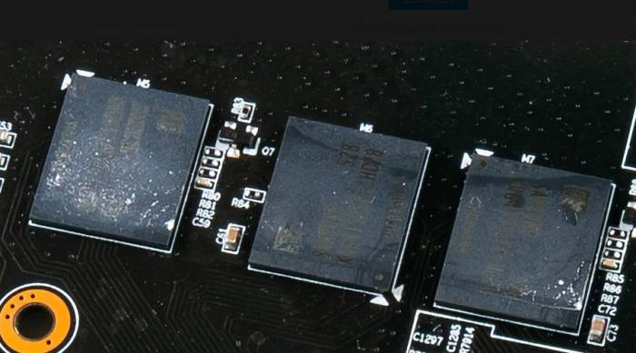
What is TSV? TSV, full name Through Silicon Via, is a new type of three-dimensional stacking packaging technology, mainly stacking multiple chips (or wafers) vertically together, and then drilling holes, passing through, and filling with metal inside to achieve electrical connection between multiple layers of chips. Compared with the traditional wire connection of multiple chips packaging method, TSV can greatly reduce the use of wires in semiconductor design, reduce process complexity, and thus improve speed, reduce power consumption, and reduce volume.
This technology can not only be used in the DRAM field but also has a broad prospect in NAND and CIS. It was first practiced on flash memory: Toshiba launched a NAND flash memory chip with 8 stacked chips in April 2007, followed by Hynix launching a NAND flash memory chip with 24 stacked chips in September 2007.In 2009, Elpida announced that it had successfully developed the industry's first TSV DRAM chip, which was stacked and packaged with 8 pieces of 1GB DDR3 SDRAM, and began to deliver samples in June 2011, marking the official entry of TSV technology into the memory stage.
Following closely behind were South Korean and American manufacturers. In March 2011, SK Hynix announced the successful development of 16GB DDR3 memory with TSV technology (40nm level). In September, Samsung Electronics launched 3D stacked 32GB DDR3 based on TSV technology (30nm level). In October, Samsung Electronics and Micron Technology jointly announced the launch of Hybrid Memory Cube (HMC) technology based on TSV technology.
After acquiring ATI, AMD had already set its sights on video memory. However, it was obviously not enough for its GPU department to develop a completely new video memory standard in isolation. Therefore, AMD brought in several crucial partners: Hynix, which had experience in 3D stacked memory, UMC, which made the silicon interposer, and the packaging and testing companies ASE and Amkor.
HBM was born as a result. As previously mentioned, GDDR had encountered bottlenecks in memory bandwidth and power consumption control. The idea of HBM was to use TSV technology to create a three-dimensional stacked video memory particle, allowing the "bungalow" to evolve into a "building". At the same time, through the silicon interposer, the video memory was connected to the GPU core and packaged together, completing the improvement of video memory bandwidth and transmission speed, which can be described as killing two birds with one stone.
In 2013, after years of research and development, AMD and SK Hynix finally launched this new technology of HBM, which was also set as the JESD235 industry standard. The working frequency of HBM1 is about 1600 Mbps, the drain power supply voltage is 1.2V, the chip density is 2Gb (4-hi), and its bandwidth is 4096 bits, far exceeding the 512 bits of GDDR5.
In addition to bandwidth, the impact of HBM on DRAM power consumption is also very important. At the same time, the R9 290X spent 15-20% of its 250W rated power consumption on DRAM, that is, about 38-50W of power consumption. The bandwidth per watt of power consumption of GDDR5 is 10.66GB/second, while the bandwidth per watt of HBM is more than 35GB/second, and the power efficiency has been improved by three times.
In addition, because the GPU core and video memory are packaged together, it can also reduce the pressure of heat dissipation to a certain extent. The original large area of heat dissipation is concentrated in a small area, and heat dissipation only needs to be targeted at this part of the area. The original design of three fans can be simplified to dual fans or even single fans, indirectly reducing the size of the graphics card.
Anyway, there are countless benefits. Whether it is AMD and SK Hynix, or the media and many players, they all believe that this is the future of video memory. The GDDR led by NVIDIA is outdated and will be swept into the dustbin of history.
The downside is that the flagship graphics card mentioned in the previous text only supports 4GB of video memory, which is a problem. After all, high bandwidth is used for high-resolution, and the reduction in the size of video memory directly makes HBM lose its practical significance.
The price is the last straw that overwhelmed AMD: The cost of HBM1 is already unverifiable, but the cost of 8GB HBM2 is about 150 US dollars, and the cost of the silicon interposer is about 25 US dollars, totaling 175 US dollars. At the same time, 8GB GDDR5 only costs 52 US dollars. Without considering the packaging and testing, the cost of HBM is already about three times that of GDDR. The retail price of a RX Vega 56 is only 400 US dollars, and half of the cost is spent on video memory. The GPU department was originally supposed to subsidize the CPU department, but now the situation has reversed. Who can afford it?As a result, AMD hastily canceled its subsequent plans to equip its graphics cards with HBM memory, and obediently followed NVIDIA's pace, directly switching to GDDR6 memory in the RX 5000 series, marking the end of HBM's second generation on AMD's gaming graphics cards.
In contrast, NVIDIA was well-prepared. In April 2016, NVIDIA released the Tesla P100 graphics card, which is equipped with 16GB of HBM2 memory, with a bandwidth of up to 720GB/s, and has a peak artificial intelligence computing performance of 21 Teraflops.
NVIDIA did not delve into HBM for many years like AMD, so how did it suddenly launch a graphics card equipped with HBM2 and sound the horn of counterattack against AMD?
The reasons behind this are quite complex. The HBM2 memory used in the Tesla P100 graphics card did not come from AMD's partner SK Hynix, but from Samsung Electronics, a South Korean company. It is not much inferior to Hynix in the development of 3D stacked memory based on TSV technology. In the case of catching up, it quickly narrowed the gap, and NVIDIA just had the intention to develop graphics cards related to HBM, and the two hit it off.
As for the silicon interposer and 2.5D packaging that AMD and companies like UMC, ASE, and Amkor finally figured out, NVIDIA found another big player in the industry - TSMC, and was attracted by its advanced packaging technology CoWoS (Chip-on-Wafer-on-Substrate). It launched this technology as early as 2011 and first applied it to Xilinx's FPGA in 2012, and the two also hit it off.
The subsequent story is self-evident. NVIDIA's graphics cards from P100 to V100, from A100 to H100, have almost become essential tools for AI training, with shipments increasing, even surpassing the traditional gaming graphics card business, and HBM has also shone in it, becoming the most dazzling gemstone.
Getting up early and arriving late is the best summary of AMD's HBM. It not only failed to counterattack NVIDIA in the gaming graphics card market with HBM, but was also used by NVIDIA to consolidate its position in the field of AI computing, and was picked by others for ripe and sweet peaches.
Three companies share memory.
While AMD and NVIDIA, the two GPU manufacturers, are competing, three leading memory manufacturers are not idle and have started the process of chasing each other in the HBM market.
In 2013, SK Hynix announced the successful development of HBM1, defining this memory standard, but like AMD, the advantage it finally obtained was not maintained for too long.In January 2016, Samsung announced the mass production of 4GB HBM2 DRAM and began production of 8GB HBM2 DRAM within the same year. It caught up with and surpassed its domestic peers, doubling the memory bandwidth compared to HBM1.
In the second half of 2017, SK Hynix's HBM2 came to the market late, finally announcing mass production; in January 2018, Samsung announced the mass production of the second-generation 8GB HBM2 "Aquabolt."
At the end of 2018, JEDEC introduced the HBM2E specification to support increased bandwidth and capacity. When the transfer rate rises to 3.6Gbps per pin, HBM2E can achieve a memory bandwidth of 461GB/s per stack. In addition, HBM2E supports up to 12 stacks of DRAM, with a memory capacity of up to 24GB per stack. Compared with HBM2, HBM2E has more advanced technology, a wider range of applications, faster speed, and larger capacity.
In August 2019, SK Hynix announced the successful development of the new generation "HBM2E"; in February 2020, Samsung officially announced the launch of its 16GB HBM2E product "Flashbolt," which began mass production in the first half of 2020.
In January 2022, the JEDEC organization officially released the standard specification for the new generation of high-bandwidth memory HBM3, continuing to expand and upgrade in various aspects such as storage density, bandwidth, channels, reliability, and energy efficiency. Its transfer data rate has doubled again on the basis of HBM2, with a transfer rate of 6.4Gbps per pin, and a single maximum bandwidth of up to 819GB/s with a 1024-bit width.
SK Hynix had already released the world's first HBM3 in October 2021 and officially started mass production in June 2022, supplying Nvidia, defeating Samsung, and once again gaining technical and market advantages in HBM.
Naturally, Samsung is not willing to be outdone. In its release roadmap, the HBM3 technology has been mass-produced in 2022, and large-scale production will start in the second half of 2023. It is expected to achieve the next-generation HBM technology with an interface speed of up to 7.2Gbps in 2024 - HBM3p, which will further increase the data transfer rate by 10%, thus increasing the total bandwidth of the stack to more than 5TB/s.
Speaking of this, everyone will inevitably have doubts. It is said that there are three companies sharing the memory market, but Samsung and Hynix together are only two, and they are all from South Korea. Where is the other one?
Micron, based in the United States, certainly did not ignore the memory market. As the acquirer of Elpida, it is not unfamiliar with 3D stacked TSV technology and even had many advantages in TSV technology before the release of HBM.
However, Micron did not follow AMD or Nvidia to develop HBM technology but chose to cooperate with Intel to develop HMC (Hybrid Memory) technology. Although it also used TSV, it has its own controller chip and is completely packaged on the PCB substrate, which is completely different from HBM and completely incompatible.In September 2011, Micron officially announced the first generation of HMC and mass-produced the second generation of HMC in September 2013. However, there were very few respondents. The first processor to adopt HMC memory was Fujitsu's SPARC64 XIfx, which was equipped with Fujitsu's PRIMEHPC FX100 supercomputer launched in 2015. Since then, it has rarely appeared in various products.
With Micron's official announcement in August 2018 to give up HMC, it hurriedly turned to the development of GDDR6 and HBM products. Fortunately, the foundation of 3D stacking technology is still there, so it is not completely behind the two Korean factories. In 2020, Micron officially stated that it would start providing HBM2 products for high-performance graphics cards, server processors, and other products. It is expected in its financial report that it will mass-produce HBM3 products in the first quarter of 2024, finally catching up with the current leading competitors.
The AI tide is still sweeping the world, and Nvidia's H100 and A100 graphics cards are still hot. As a new piece of the memory market, HBM is the most delicious piece. Chip industry consulting firm SemiAnalysis said that the price of HBM is about five times that of standard DRAM chips, bringing greater total profits to manufacturers. At present, HBM accounts for less than 5% of global memory revenue, but SemiAnalysis projects that it will account for more than 20% of total revenue by 2026.
Most of this delicious cake is left to the pioneers. According to the survey by TrendForce Consulting, the market share of the three major original factories of HBM in 2022 is SK Hynix 50%, Samsung about 40%, and Micron about 10%. Micron believes that its products are not inferior to Korean factories, but the market will never make an exception for a manufacturer who prides itself on technological leadership.
Summary
At that time, Sakae Okamoto of Elpida believed that Japan's semiconductors lost people but not the battle. At the time of the interview, Micron CEO Mark Durcan also said that the AI field not only includes HBM but also high-density DDR5, Micron's custom LP DRAM, and some graphics memory. In summary, it lost HBM but has not yet admitted defeat in AI.
If these two CEOs summarize the lessons of failure, they can only sigh, "It's time, fate, and luck, not what I can do." Of course, they can't lose. Micron and Elpida will not say that technology is not good even if they go bankrupt, and they attribute the fault to the market, leaving a relaxed body.
Looking back, was AMD's judgment wrong when it released the R9 Fury X in 2015? Of course, it's not wrong. The memory bandwidth has indeed reached a bottleneck. There is almost no progress from GDDR5 to GDDR6X. However, in gaming graphics cards, large caches can be used as frame buffers, allowing the cheaper GDDR to continue on the road. But in the data center and AI accelerator cards, the bandwidth problem is indispensable for HBM, and cost has become the least noticeable issue in this field.
Now, AMD has turned around and is fighting in the AI field again, hoping that HBM will help them soar in this market.
Leave A Comment