Can it catch up with TSMC in five years?
When Samsung finally manages to resolve the yield issues of 3nm, it will surely recall the afternoon when it launched the world's first 14nm mobile processor.
In June last year, Samsung announced the official production of 3nm chips, becoming the only global semiconductor manufacturer to adopt GAA (Gate-All-Around) transistor technology and provide 3nm process foundry services.
Some say that by surpassing Intel and TSMC to mass-produce 3nm in advance, Samsung has once again taken the lead and once again proved the strength of the Korean semiconductor industry. The minor setbacks in 4nm and 5nm do not affect the overall situation.
However, after the simple good news was released, the bad news followed: some media reported that the yield of the production was too low, and the scale of the first batch of mass-produced chips was small. In the short term, there were no major customers willing to pay, and the so-called mass production was equivalent to losing money to make a fuss, with a clear gap compared to the old rival TSMC.
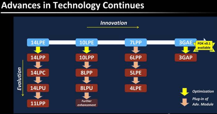
Facing various doubts from the outside world, Samsung was very low-key until recently, saying that the yield of the improved 3nm process mass production has reached 60%-70%. In the latest roadmap, Samsung plans to mass-produce the second-generation 3nm process (3GAP) next year and the 2nm process (SF2) in 2025.
Advertisement
But this has also aroused more people's concerns. TSMC is about to mass-produce 3nm Apple chips on a large scale, but Samsung has not yet come up with a plan for mass production of 3nm chips on a large scale. Is its yield really in line with customer expectations? Can the second-generation 3nm process really defeat TSMC's N3? Will major customers such as Qualcomm, AMD, and Nvidia really change their minds at the 3nm node?
Continuing to improve the existing 4nm process and missing the 3nm battle in 2023 is the most stable and reasonable choice for Samsung's semiconductor department. It's just that avoiding the battle completely lacks the courage to invest against the cycle at the beginning.
Samsung 14nm - the beginning of overtaking on the bend
"Samsung's advanced 14-nanometer FinFET process technology is undoubtedly the industry's most advanced logic process technology," said the executive vice president of sales and marketing at Samsung's system LSI department. "We hope that the production of our 14-nanometer mobile application processors can further improve the performance of flagship smartphones and have a positive impact on the development of the mobile industry."
It is not difficult to feel the pride of this Samsung department leader from the words of the press release. When manufacturers such as Qualcomm, Apple, and MediaTek are still using TSMC's 20nm process, Samsung's Exynos processor can take the lead and use the 14nm process one year earlier. In terms of both performance and power consumption ratio, it can defeat the flagship mobile processors of the same period with an overwhelming advantage.His confidence naturally stems from Samsung's semiconductor division's 14nm process, but this process is indeed hard-earned.
As part of the Four Asian Tigers, Singapore, Taiwan, and South Korea, these three little dragons, in the booming semiconductor industry, all chose to vigorously introduce and support locally, attracting a large number of American and European semiconductor manufacturers to set up factories. After taking over this part of the industry, some excellent local manufacturers also took the opportunity to rise. Taiwan's TSMC and South Korea's Samsung Electronics are the outstanding representatives among numerous local manufacturers.
Samsung Electronics has prospered by heavily betting on storage, while TSMC has been unyielding in wafer foundry. At the beginning of their start, the two companies chose two different tracks.
With the bankruptcy of Germany's Qimonda and Japan's Elpida, Samsung Semiconductor has reached the ceiling in the storage market. Just at this time, the rise of smartphones has made Taiwan's semiconductor manufacturers, led by TSMC, shine brightly, relying on wafer foundry to make a fortune. How can people not be tempted?
Coincidentally, in 2005, the global storage market plummeted. In order to reduce losses for the semiconductor division, Samsung took the opportunity and officially started the wafer foundry business in this year.
However, Samsung has always been half a step behind TSMC in process technology. TSMC is not only the first manufacturer to use immersion lithography to produce 90nm chips, but also the first in the world to launch 28nm general process technology. At the key node of 28nm, TSMC has occupied the top position in the market share for many years. The early high-end processors of smartphones, such as Qualcomm Snapdragon 800 and MediaTek's MT6589T, all use TSMC's 28nm process.
Although Samsung also has its own wafer factory, it is far from TSMC in terms of process iteration. In 2005, Samsung started with 90nm and took over Qualcomm's CDMA chip orders, while TSMC had already started trial production of 65nm chips. The objective technical gap, coupled with Samsung's lack of focus, has kept its foundry business at a small scale. From 2005 to 2009, Samsung's foundry business revenue never exceeded $400 million, while TSMC had already approached $10 billion.
However, Samsung's foundry division is not without achievements. During this period, Samsung approached Steve Jobs, starting with the flash memory of the iPod Shuffle in 2005, and manufactured various chips for Apple, including the iPhone launched in 2007, which carried Samsung's S5L8900 and used Samsung's 90nm process technology. Three years later, on the iPhone 4, although Apple launched its first self-developed chip A4, its core layout was very similar to Samsung's S5PC110, and it used Samsung's 45nm process, including the subsequent A5, A5X, A6, A6X, A7, all of which were contracted to Samsung for foundry.
The global sales of the iPhone not only set one record after another for Apple, but also made Samsung's ranking in the wafer foundry market soar rapidly from the top ten in 2007 to the fourth in 2012, with foundry revenue of $3.439 billion, only behind TSMC, GlobalFoundries, and UMC, becoming an important player in the foundry market. It can be said that without Apple, there would be no Samsung wafer foundry business today.Success and failure both lie with Apple. As a huge consumer electronics conglomerate, Samsung Electronics not only manufactures chips for Apple but also provides flash memory, storage, screens, and other components. Moreover, Samsung's mobile phones also compete with iPhones in the smartphone market. Samsung, which is both in the limelight and behind the scenes, is not the most ideal partner. Moreover, the lesson of HTC being cut off from Samsung's AMOLED screens is also a warning to Apple.
Moreover, at this time, the leader in wafer foundry - TSMC not only took the lead in 2011 to conquer the 28nm process but also quickly advanced to the 20nm process. Apple, which pursues performance and power consumption, immediately clicked with TSMC. In the 2014 iPhone 6 series, it abandoned the friend and foe Samsung and handed over the entire A8 chip foundry to TSMC. Once the news came out, Samsung's stock price plummeted instantly.
Samsung is not completely unaware of the rumors from the outside world. Since 2011, Apple and TSMC have been secretly colluding, exchanging glances all day long. As the foundry for Apple's chips, Samsung also made a tough statement when receiving stock analysts after learning this news: as long as TSMC dares to do (Apple's chips), it will definitely dare to sue.
Facing various difficulties, TSMC, the world's largest wafer foundry, also took out all its tricks to attract Apple.
In response to the potential problem of insufficient production capacity after taking Apple's order, TSMC invested heavily in building and expanding production lines with a $9 billion investment: TSMC's 15th factory in Taichung started construction on July 16, 2010, and the plant was completed in early 2012; in the first half and second half of 2013, it expanded its Hsinchu 12th factory and Nantze 14th factory. Among them, the Hsinchu 12th factory even opened a "Apple exclusive" 20nm A8 chip R&D production line, and a large number of production line engineers were dispatched from the Nantze 14th factory to cooperate.
In response to the chip IP disputes between Samsung and Apple, TSMC sent nearly a hundred people of the "One Team" to Apple's headquarters in the United States at the end of 2011 to help Apple solve the design and patent certification issues of the A6 chip. It also provided two versions of the A8 plan for Apple to choose from before 2014, maximizing the help to Apple to reduce the risk of IP lawsuits with Samsung.
Finally, in the 2014 Apple launch, the A8 chip on the iPhone 6 and iPhone 6 Plus was quietly changed from Samsung to TSMC. TSMC finally squeezed out Samsung and enjoyed the order of hundreds of millions of mobile phone chips alone.
Seeing that it is no longer possible to retain Apple, and the lawsuit is unlikely to curb TSMC in the short term, Samsung came up with another plan, which is to accept the advice of Liang Mengsong, a veteran of TSMC's R&D, to skip the 20nm and 16nm nodes after 28nm, and sprint to the 14nm node. In the traditional planar field effect tube size to the limit, it fully promotes the landing of FinFET technology, realizing the three-dimensional field effect tube, turning the impossible into possible, and finally achieving overtaking.
In fact, Samsung has long been plotting the fat of wafer foundry. At the highest decision-making meeting of Samsung in 2009, a plan - Kill Taiwan (kill Taiwan) - was secretly passed, and one of the targets of this plan is the foundry giant TSMC.
According to media decryption, since 2009, Samsung has taken away 50 middle and senior R&D executives from TSMC. In order to strengthen the strength of wafer foundry, Samsung's poaching also targeted talents from the world's top semiconductor companies. People familiar with Samsung pointed out, "When Samsung poaches, it will first sign a three-year contract, ensuring that the salary is at least twice that of the original company. After three years, it will renegotiate based on performance."The arrival of a large number of semiconductor talents and the influx of a huge amount of R&D funds have finally enabled Samsung to achieve what others thought was an almost impossible overtaking. While TSMC was still delighted with the mass production of 20nm at the beginning of 2014, Samsung announced the official launch of its 14nm FinFET process at the end of 2014.
When the 14nm-based Exynos 7420 was released and officially launched, not only TSMC and Apple, which had just reached a cooperation, but all wafer foundries were stunned. Everyone was still struggling with 20nm, but this Korean tycoon, who had been in the industry for not long, had advanced half a year earlier with 14nm. Could it be that Intel and TSMC had given Samsung a head start in tutoring?
And DRAM practitioners have long been accustomed to it. Samsung Semiconductor was also like this. Not only did it use counter-cyclical investment to overtake in the red sea of the DRAM market, but it also took the lead in launching the world's first 64Mb DRAM in 1992. It also used counter-cyclical investment to kill off Qimonda and Elpida, and finally laughed at the end. This time, it's finally the turn of wafer foundries.
Not only that, but starting with Samsung's 14nm, the most brutal round of reshuffling in the history of wafer foundries officially began: if you can solve FinFET, you can enjoy a good life every night, if you can't solve it, you can play mud with 28nm and older processes.
Samsung's 5nm - the failure caused by radicalism
At least one generation ahead of TSMC's 20nm process, Samsung successfully attracted the attention of a large number of fabless manufacturers, including Apple.
TSMC was even more on guard, and founder Zhang Zhongmou made a comeback, preparing the Night Owl Plan in 2014, which was called "100,000 young people, 100,000 livers, one liver per person to save Taiwan". It selected elite engineers to accelerate the development of the 10nm process in a 24-hour three-shift rotation.
However, the lag behind in FinFET has become a foregone conclusion, and more fatally, the 20nm process launched in 2015 completely exposed the shortcomings of the process on the flagship processor Qualcomm Snapdragon 810. Both heat generation and power consumption reached a shocking level. In that year, except for the Samsung Galaxy S6 series and Note 5 equipped with Exynos 7420, all major Android manufacturers without exception had a complete failure.
As a result, Apple also began to make its own small calculations: although it parted ways with Samsung, now looking back, TSMC is not as good as imagined. If the price is right, it is also possible to reconcile with Samsung and make up for the past.
Therefore, in the iPhone 6s series, Apple unprecedentedly used dual suppliers for processors, with the A9 processor using Samsung's 14nm and TSMC's 16nm processes. This is the same as the iPhone 12 using multiple screen suppliers in the future, which not only ensures the stability of supply but also allows Apple to take the initiative in price negotiations through this method, and minimize costs to the greatest extent.On the iPhone 6s, the performance and power consumption differences between the chips from Samsung and TSMC (Taiwan Semiconductor Manufacturing Company) caused quite a stir, with many users and websites reporting that the Samsung version of the iPhone 6s had significantly weaker battery life than the TSMC version. This led to a trend of returning Samsung chips and buying TSMC ones, and to this day, there are still many people sharing tips on how to identify the chip version.
Which is better, Samsung's 14nm process or TSMC's 16nm process? Most people might lean towards the latter, and Apple is no exception. This chip controversy also firmly placed Apple on TSMC's side, making it the sole foundry for its processors.
However, Samsung has thoroughly proven its wafer foundry strength through the 14nm process. The gap in performance and power consumption can be completely offset by relatively cheaper foundry prices. Processor manufacturers such as Qualcomm also extended an olive branch to Samsung in 2016, entrusting the flagship processor Snapdragon 820 to Samsung for foundry production, and a large number of manufacturers began to recognize Samsung's wafer foundry capabilities.
As for why TSMC is still facing a formidable challenge despite its 16nm process being on par or even surpassing Samsung's 14nm, the answer emerged in 2017: that year, the Qualcomm Snapdragon 835 used Samsung's 10nm process, while the contemporary Apple A10 still used TSMC's 16nm process. Apart from Apple's pride in single-core scores, it lagged behind the Snapdragon 835 in terms of energy consumption and multi-core performance, and TSMC was indeed half a step behind.
In fact, when xxnm becomes a numerical code, the most effective way to test the reality of the process is the actual foundry products. After 2014, mobile processors began a major iteration once a year, and feedback from consumers made the pros and cons of new processes undeniable, and the competition between Samsung and TSMC gradually moved from behind the scenes to the forefront.
Starting from 10nm, Samsung and TSMC have been in fierce competition: in September 2018, the Apple A12 chip was released, using TSMC's 7nm process; in December 2018, the Qualcomm Snapdragon 855 was released, using Samsung's 7nm process. The two chips did not show much difference in energy consumption, and the two companies almost tied in the 7nm process.
To ensure an advantage, Samsung also very aggressively introduced EUV (Extreme Ultraviolet) process at 7nm to improve production efficiency, once again leading TSMC's first-generation 7nm DUV (Deep Ultraviolet) process.
However, at the key node of 5nm, Samsung's foundry department made a fatal mistake, completely ruining the good situation that had been formed since 2015 and falling behind TSMC again.
What mistake was that? It is that Samsung's 5nm is not a complete upgrade from one node to another compared to 7nm, but an upgrade based on the original 7nm. Many people pointed out that Samsung was "hanging a sheep's head and selling dog meat," marking 6nm as 5nm, and forcibly renaming it to catch up with TSMC's progress.
In Samsung's roadmap, it is obviously divided by the four key nodes of 14-10-7-3. Samsung originally planned to adopt a brand-new GAA (Gate-All-Around) structure at 3nm to surpass TSMC again and take a leading position in technology.The specific technical details that can be inferred from the outside world also provide a glimpse into the truth. In terms of transistor density, TSMC's N5 process has a density of 173.1 MTr/mm², while Samsung's 5LPE process has a density of 126.5 MTr/mm². Although they are in the same order of magnitude, there is a significant gap between them, which indirectly proves that Samsung's 5nm is not a complete iteration.
Some may wonder, Samsung was able to closely pursue TSMC in the early stages of FinFET, taking away many of TSMC's original customers. At key nodes such as 10nm and 7nm, it could still compete with TSMC on an equal footing. Why did it suddenly fall behind at 5nm?
The reason may be seen from the market share. From 2019 to 2022, TSMC has always firmly occupied half of the foundry market, while Samsung, although ranking second, has not seen the gap with TSMC narrow. As of the fourth quarter of last year, TSMC accounted for 58.5% of the share, and Samsung Electronics accounted for 15.8%, with a market share gap of 42.7%, higher than the previous quarter's 40.6%, and the gap between the two has not narrowed.
In terms of R&D investment, the gap between Samsung and TSMC is even more obvious. While TSMC has been increasing its investment for several consecutive years, Samsung has tightened its investment in wafer foundry, only about one-third of TSMC's.
Under such circumstances, Samsung's own customer base is also very limited. TSMC has long had stable big customers such as Apple, Broadcom, HiSilicon, AMD, MediaTek, Nvidia, Qualcomm, and Intel, while Samsung's production capacity relies on its own Exynos chip digestion, and other production capacities are mainly allocated to Qualcomm, with other customers such as Nvidia, IBM, and Intel accounting for a very small proportion.
It seems that Samsung was in the limelight from 14nm to 7nm, as the only two advanced process foundries, attracting a large number of customers to place orders. In fact, it was walking on a tightrope, catching up with TSMC's pace in advanced processes with about 30% of revenue and R&D funds, and any slight mistake could lead to a disastrous situation.
In addition, after losing Apple, the largest consumer electronics customer, it means that tens of billions of dollars are lost every year. It has almost become a fantasy for Samsung to want to turn the tables on TSMC after 2015, and using the 3nm with GAA is more like the ingenious plan proposed by Wei Yan of Shu Han in the Zishi Valley. In front of TSMC's already mature 4nm and 5nm, how much advantage there is in yield and transistor density is only known to the Samsung engineers who are operating the knife.
The anti-cycle failure under the siege of three sides
Although Samsung's semiconductor business is huge, the main departments are divided into three, namely memory, system LSI, and wafer foundry, among which memory is the crystallization of the efforts of two generations of Korean semiconductor talents. From the 1990s to the present, it has maintained the position of leading the storage industry and is also the department that Samsung is proud of for its anti-cycle performance.
But now the storage market is still in the cold winter, advanced processes are repeatedly frustrated, and Exynos has been relegated to the cold palace by its own flagship, which can be described as being besieged on three sides. The three major semiconductor businesses have encountered major problems at the same time. If handled improperly, it will trigger a chain reaction of neglecting one thing for another. It is important to know that even in the most skilled storage business, Samsung is not invincible. Hynix, Micron, and domestic storage are still eyeing it. Once the investment slows down, the market may change hands in an instant. As for the Exynos chip, the only highlight moment can be traced back to eight years ago. If it dawdles any longer, it will lose the qualification to be a flagship mobile chip.The year 2023 has presented Samsung's semiconductor division with an unprecedented predicament that has not been seen for over a decade. Now, if Samsung wishes to wield the heavy stick of counter-cyclical investment once more, it must carefully weigh the importance of its three main departments and the urgency of the situation. Even with Samsung's vast resources, it cannot afford to squander them without discretion.
On May 24th last year, Samsung Electronics announced that it would invest 450 trillion won (approximately 36 billion US dollars) over the next five years to accelerate the development of semiconductors, biopharmaceuticals, IT, and other next-generation technologies, in response to the increasingly severe economic and supply chain shocks.
Many might think that now, Samsung's foundry business will finally rise to prominence. However, it's too early to celebrate. Out of the 36 billion dollars, just how much will the semiconductor division receive, and how much will the foundry business get? When spread over five years, whether it can surpass TSMC and Intel's R&D investment in foundry services is still up for debate.
Considering Samsung's previous investment ratios in its memory business and foundry operations, the situation is probably not as simple as many people imagine, and the gap with TSMC is not so easily bridged.
It seems that Samsung's foundry division has also come to terms with the reality that memory is the favored child, while it is merely the second son, and has become more pragmatic. In recent speeches, senior executives stated that TSMC is far ahead of Samsung in chip manufacturing and that it will take five years to catch up and surpass TSMC, objectively acknowledging the gap between the two.
But the problem is, they also believe that the GAA (Gate-All-Around) technology that Samsung is about to adopt is crucial. When TSMC transitions to 2nm, Samsung's lagging situation will change, and they predict that TSMC will encounter difficulties in R&D due to this new technology.
Still pinning hopes on the premise that their competitors will make mistakes, Samsung's semiconductor division may be overly optimistic.
Leave A Comment