Google chip, is it experiencing an Apple moment?
On October 19, 2021, at an autumn press conference, the flagship smartphone Pixel 6 series, equipped with Google's first self-developed chip Tensor, made its debut, unveiling its mysterious veil and leaving more space for people's imagination.
Google Senior Vice President Rick Osterloh said at the conference that this chip is "the biggest mobile hardware innovation in the company's history", and Google CEO Sundar Pichai had already posted a photo of the Tensor chip on Twitter, showing his pride in the self-developed project.
It took Google a full four years from the beginning of research and development to the final mass production. When we look back at Google's development history, we will find that the development trajectory of Tensor is always centered around the Pixel mobile phone, and it is appropriate to describe them as two sides of the same coin.
Looking back carefully, there are only a few mobile phone manufacturers in the world that are still sticking to self-developed chips, only Google and Apple are still moving forward on this road. Apple needs no further explanation, what supports Google to keep burning money on chips?
Advertisement
Pixel means pixel, and Tensor represents tensor. These two words outline Google's dream of self-developed mobile chips.
Multi-core in one machine
It is strange to say, before 2017, Google did not have a real mobile phone team.
Although as early as January 2010, Google launched its first self-branded mobile phone, Nexus One, in partnership with HTC, but in a long period of seven years, Google, who has been close to LG, flirted with Samsung, called brothers with Motorola, and held hands with Huawei, did not have a complete mobile phone research and development team.
On the back cover of all Nexus mobile phones, not only is the word Google printed, but also the logo of other brands is engraved. It is better to say that this is Google's version of the ODM mobile phone. Google is responsible for printing, adapting the system, and proposing a bunch of design requirements, while other manufacturers are responsible for producing mobile phones.As for Motorola Mobility, which Google once spent a staggering $12.5 billion to acquire, it never became the core of the business. Immediately after the acquisition, Google took a hatchet to it, laying off employees worldwide, streamlining product lines, closing offices and research and development centers, exiting unprofitable markets, and selling factories and non-core businesses... Other companies build upon their acquisitions, but Google began to dig at the roots.
After absorbing and digesting 17,000 patents, Google resold Motorola Mobility to Lenovo in 2014. The company that produced the first mobile phone did not leave Google with much of a hardware legacy. At this point, Google seemed somewhat detached from the world, watching as many manufacturers fought fiercely in the mobile phone market, while it focused on the software field, occasionally incubating one or two astonishing new projects internally, such as the modular phone that once attracted worldwide attention.
However, as time moved forward to 2016, the situation was different. When Google saw the mobile phone market rising steadily and profits were abundant, it couldn't help but be tempted, especially in the North American market, where Samsung's high-end Android flagship was the only one, and the market share of other manufacturers was rapidly shrinking. This opportunity presented itself, prompting Google to rethink the possibility of integrating hardware and software.
In April 2016, Google recruited Rick Osterloh, the global president of Motorola, to serve as the head of hardware, officially launching the self-developed mobile phone project. This time, the target was the high-end mobile phone market, especially Apple's iPhone. Osterloh did not conceal Google's ambitions in this area in the interview: "Our focus is to strive to bring users into the Android ecosystem, especially in the high-end market."
In October 2016, the Google Pixel phone made its debut. Pixel, which means pixel, represents the powerful imaging capabilities of this phone. At the launch, Google emphasized that DxOMark rated Pixel as the best smartphone camera of the year, thanks to Google's improved HDR+ technology. On the Google Pixel, the camera app captures a photo buffer as soon as the user opens it, significantly reducing shutter lag and greatly improving the user's shooting experience.
Due to the somewhat hasty launch of the first generation of Pixel, the sales were not satisfactory, but the failure did not discourage Google. The feedback from this phone instead strengthened its confidence to continue with the new hardware strategy. In September 2017, Google acquired HTC's mobile device department, which was the contract manufacturer for Pixel, for $1.1 billion, fully betting on the upcoming new Pixel phone.
In October 2017, the Pixel 2 series was officially released. Compared with the previous generation of Pixel, the hardware upgrades were not many, but in Google's official press release, one thing was emphasized: not only does the Pixel 2 and Pixel 2 XL have a Samsung-manufactured SoC, but also a co-processor developed by Google itself - PVC (Pixel Visual Core).
Google said that the Pixel 2 camera is equipped with excellent hardware, software, and machine learning. Users only need to aim the camera and shoot to take amazing photos and videos. HDR+ is one of the technologies that help take excellent photos, allowing users to take excellent photos in scenes with a large range of brightness, from dimly lit landscapes to sunny skies. In order to expand the application range of HDR+, to handle the most challenging imaging and machine learning applications, and to provide lower latency and more power-efficient HDR+ processing, PVC was born.
In terms of specific hardware, the core of PVC is Google's image processing unit (IPU), which has 8 custom-designed cores by Google, each with 512 arithmetic logic units (ALU). When used on a mobile phone, it can provide raw performance of more than 3 trillion calculations per second.The improvement in photography is even more significant. Google's official data shows that through PVC, the running speed of HDR+ can be 5 times faster than running on an application processor (AP), while the power consumption is less than one-tenth.
This processor caused quite a sensation at the time. Previously, everyone's thinking was limited to optimizing the ISP of mobile phone processors. If a more powerful and lower power-consuming chip could replace the built-in ISP, wouldn't the improvement in mobile imaging be easy to achieve?
This idea greatly influenced domestic mobile phone manufacturers, such as OPPO's MariSilicon X, Xiaomi's Surge C1, and vivo's V1... Manufacturers have successively started to explore self-developed ISPs. Google led the trend for a while and also won the championship in mobile imaging competitions for several years in a row. The Pixel 2 and Pixel 3 achieved 98 and 101 points in DxOMark mobile imaging scores, and the latter tied with the iPhone XR in single-lens mobile imaging, proving the feasibility of self-developed chips.
Multiple cores in one machine has become one of the symbols of Google Pixel phones. Everyone, including mobile phone manufacturers, is curious about how Google, which rarely participated in hardware research and development before, suddenly came up with such a big move like PVC? Is there a high-level person guiding behind the scenes?
The road to self-development is long and arduous.
Google's Pixel Visual Core did not stand on the shoulders of giants, because it is already a small giant itself.
Google's self-development began in 2013. At that time, Jeff Dean, the head of Google AI, calculated that if 100 million Android users used the mobile phone voice-to-text service for 3 minutes a day, the computing power consumed would be twice the total computing power of all Google data centers, and the global Android users are far more than 100 million.
The scale of data centers cannot expand indefinitely, and Google cannot limit the time users use the service. At this time, another way out must be found. However, neither CPUs nor GPUs can meet Google's needs: CPUs can only handle a relatively small amount of tasks at a time, and GPUs have lower efficiency when executing a single task, and the range of tasks they can handle is smaller.
Google ultimately chose to forge a new path and set a high goal: to build a domain-specific architecture for the purpose of machine learning, and to reduce the total cost of ownership (TCO) of deep neural network inference to one-tenth of the original.
In 2014, Google TPU (Tensor Processing Unit) officially began research and development. Thanks to Google's strong scientific research strength and outstanding chip talents recruited from various companies, the development of TPU was very smooth. It started to be deployed and applied in data centers only 15 months later, and its performance per watt reached 30 times that of GPUs and 80 times that of CPUs.Google has been quite low-key about this matter until the 2016 Google I/O Developer Conference, where CEO Sundar Pichai officially unveiled the TPU, a self-developed achievement, to the world.
Pichai proudly stated that the AlphaGo developed by DeepMind could defeat South Korean Go player Lee Sedol, and the TPU in the underlying hardware was indispensable. The TPU is like the woman in Greek mythology who triggered the Trojan War—Helen, and its emergence has caused "thousands of chips to compete with it."
Five years later, Sundar Pichai announced the TPU v4 at the 2021 Google I/O Developer Conference:
"The advancement of AI technology relies on the support of computing infrastructure, and the TPU is an important part of Google's computing infrastructure. The new generation of TPU v4 chips is more than twice as fast as v3. Google has built a Pod supercomputer with TPU clusters, with a single TPU v4 Pod containing 4096 v4 chips, and the interconnect bandwidth between chips in each Pod is ten times that of other interconnect technologies. Therefore, the computing power of the TPU v4 Pod can reach 1 ExaFLOP, which is 10 to the 18th power of floating-point operations per second, equivalent to the total computing power of 10 million laptops."
To this day, the TPU has become one of the representatives of Google's self-developed technology, with tens of thousands of them deployed in data centers, performing hundreds of millions of AI computing tasks.
In a sense, the TPU aims to replace accelerator cards like NVIDIA A100 and H100, and for Intel's Xeon CPUs used in servers, Google has developed another chip—Argos VCU.
In March 2021, Google first introduced a self-developed chip for YouTube servers at the ASPLOS conference, namely Argos VCU, whose task is very simple, which is to transcode videos uploaded by users.
But don't underestimate this task. Users upload more than 500 hours of various formats of video content to YouTube every minute, and Google needs to quickly convert these contents into multiple resolutions (including 144p, 240p, 360p, 480p, 720p, 1080p, 1440p, 2160p, and 4320p) and various formats (such as H.264, VP9, or AV1). Without a chip with strong encoding capabilities, fast transcoding would be impossible.
Google has tried two third-party solutions. The first is Intel's Visual Computing Accelerator (VCA), which includes three Xeon E3 CPUs, built-in Iris Pro P6300/P580GT4e integrated graphics cores, and advanced hardware encoders. The second is to use Intel Xeon processors with software encoding to complete the task.Whether it's the former or the latter, both require a massive server scale and huge power consumption, which is a burden that Google cannot bear.
Therefore, after TPU, Google started the development of VCU. Scott Silver, Google's vice president of engineering who is responsible for overseeing the huge infrastructure of YouTube, said that since 2015, a team of about 100 Google engineers has been dedicated to designing the first generation of Argos chips. In the following years, this team not only completed the development but also applied the chips in Google's data centers, and the strength of Argos has been demonstrated—it processes video 20 to 33 times more efficiently than traditional servers, and the time to process high-resolution 4K video has been reduced from several days to a few hours.
The next generation of Argos may have already quietly gone online in the server. According to reports, Google's second-generation VCU, which is self-developed, will support AV1, H.264, and VP9 codecs, which can further improve the efficiency of its encoding technology and will also be the most powerful support for the YouTube content creation ecosystem.
What is most surprising is that Google has a very clear and clear blueprint for self-developed chips. It often starts from the perspective of practical application and develops according to its own needs. Self-development is not the goal, but a clever means under the strength, and using it to complete what other chips can't do is the ultimate goal.
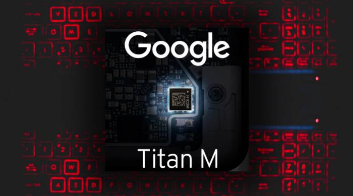
It is also based on this idea that at the Google Cloud Next '17 conference in 2017, Google launched a custom security chip called Titan, which is designed for hardware-level cloud security. It realizes safer identification and authentication by establishing an encrypted identity for specific hardware, thus preventing the increasingly rampant BIOS attacks.
Unlike the previous two chips, the Titan chip is not aimed entirely at Google itself. Its emergence is to convince companies that data stored in Google Cloud is safer than in their local data centers.
Google said that the self-developed Titan chip establishes a strong hardware-based system identity to verify system firmware and software components, protecting the boot process, all thanks to Google's own hardware logic, which fundamentally reduces the possibility of hardware backdoors. The ecosystem based on Titan also ensures that the facility only uses authorized and verifiable code, ultimately giving Google Cloud a safer reliability than local data centers.
From TPU to VCU, to Titan, Google has gradually built its own moat for the future and has successfully led a trend of large enterprises developing their own chips, with Meta, Tesla, Microsoft, Tencent, Alibaba, ByteDance, and countless other companies following Google to set sail in the sea of chips.
Google's three major self-developed chips, from 2013 to 2023, have gone through a ten-year journey, which is also a process of a confused apprentice becoming a teacher who teaches others to fish.
Mobile chips that are not satisfactory everywhereReturning to the PVC on the Pixel 2 series, it was not actually surprising that Google could come up with such a chip in 2017. After all, whether it's TPU or VCU, they have a close relationship with images. Developing a chip specifically for mobile imaging based on them can certainly achieve twice the result with half the effort.
However, the PVC did not drive the sales volume of the Pixel series. According to IDC data released by Bloomberg, the total sales volume of the first generation of Pixel was 3.3 million units, and the total sales volume of the Pixel 2 series was 4 million units, only increasing by more than 700,000 units, which is equivalent to the tail of the sales volume of high-end flagships of Samsung and Apple in the North American market that year.
But Google didn't take the sales volume to heart and continued to convert its self-developed experience in the server field to smartphones. In October 2018, the Pixel 3 series was officially released. In addition to inheriting the PVC of Pixel 2, it also used another Google self-developed chip - Titan M.
Yes, the Titan chip mentioned in the previous text was applied to Google's latest flagship one year later. This is also one of the advantages of self-development. The security chip that was once exclusive to enterprise users is now spread on every mobile terminal.
At the launch, Google stated that the Pixel 3 has become the most secure mobile phone to date, thanks to its enterprise-level security chip Titan M. Based on the Titan chip used in Google's cloud data center, Google has deeply customized it for mobile devices, thereby protecting users' security and privacy.
In fact, the Pixel 2 series has already built in a hardware structure independent of the processor, named Security Module, which also has its own Flash/RAM/processing unit and other components. Titan M is based on it, integrating the results of the Titan chip.
Titan M's protection for smartphones starts from the boot level, deeply integrating with Verified Boot, and can also help Pixel 3/XL to verify the lock screen password, limit the number of attempts for bad programs to unlock the mobile phone, and also protect third-party applications and transactions involving security sensitivity, which is a real all-rounder in the field of security.
In order to prove that Titan M is not bragging, one year later, Google directly launched a special Android security reward program: if security researchers find and prove that there are vulnerabilities in Google's self-developed Titan M security chip, they can receive a reward of up to 1 million US dollars.
It is not clear whether anyone has received this reward, but Google dares to offer a price of 1 million US dollars, which is enough to prove the reliability of Titan M. Subsequent generations of Pixel mobile phones have all carried this security chip, which has made a great contribution to the privacy and security of Pixel users.It's a pity that neither PVC nor Titan M has been of much help in boosting the sales of Pixel phones. The total sales of the Pixel 3 series reached 9 million units, mainly thanks to the mid-range Pixel 3a series, which did not feature PVC and instead helped Google to approach the threshold of 10 million sales.
However, the sales of the following two generations of Pixel phones can be described as dismal. In October 2019, the Pixel 4 series was officially released, upgrading PVC to the brand new PNC (Pixel Neural Core). Compared to PVC, PNC allows the phone to preview dual exposure and HDR+ in real-time, enabling users to see the final image before pressing the shutter. The image computing capability has been further improved, but the total sales of this generation, including the Pixel 4a series, were only about 5.5 million units, a significant decline compared to the previous generation.
The Pixel 5 was a complete disaster. As a flagship phone, it only used the Qualcomm Snapdragon 765G, without the latest PNC or PVC. Including the Pixel 5a, the final sales were a meager 2 million units, lower than the sales of the first generation, and there were even rumors that Google would shut down the Pixel production line.
This has also led to doubts about self-developed chips in mobile phones. Google has been thriving in the field of self-developed server chips, but it seems to be out of place in the mobile market. After five or six years of hard work, the total sales are still not as high as the annual sales of a single model of Apple's iPhone. Who is the problem? Google or self-development?
Looking back, both PVC and PNC exist as co-processors, and the additional cost is destined to make them irrelevant to mid-range phones. However, the highest sales are precisely in the mid-to-low-end phones, and the biggest self-developed selling point can only be left to the flagship. How to make a choice is a very painful thing.
Google Pixel, with its bumpy journey, and the self-developed chip with a difficult fate, Google has fallen into a long period of confusion.
Google's Apple Moment
After the downturn, Google's choice was to continue to spend money.
In October 2021, Google held the Pixel Autumn Release as scheduled, and the self-developed Tensor chip immediately attracted global attention. Following Apple's A series, Samsung's Exynos, and Huawei's Kirin, another mobile phone manufacturer entered the chip-making field. The performance, experience, and prospects are all issues of concern.
Although Google repeatedly emphasized the self-developed attributes of Tensor, this chip was not created by Google alone.By disassembling through TechInsights, it can be seen that the packaging size of the Tensor is 10.38mm x 10.43mm = 108.26mm², and the internal chip is labeled "S5P9845", which conforms to the traditional Samsung Exynos processor naming rules, such as the chip label of Exynos 990 is S5E9830, and the chip label of Exynos 2100 5G SoC is S5E9840. This degree of similarity can no longer be glossed over by the reason of Samsung's foundry.
In fact, around 2020, Samsung officially opened up semi-custom chip design services. According to a report by the Korean media ETNews, Samsung Electronics will manufacture semiconductor chips for Cisco Systems and Google, and is responsible for the entire semiconductor manufacturing process from design to production. Its strategy is to provide customers with the required customized technology and functions from the design phase, and Google's Tensor chip is the ultimate product of Samsung's semi-custom design.
Specifically, the hardware of Tensor and Exynos 2100 is also very similar, but Google has made some adjustments in the CPU frequency and L2 cache, and is more aggressive in the scale and frequency of the GPU. In addition, Tensor also integrates Google's self-developed ISP and TPU, and uses Samsung's baseband externally. Google's self-developed chip looks like a complete version of Exynos 2100. Even the Tensor G2 released last year is also based on the Tensor, with only minor modifications and no major changes.
At this time, there is a question, whether completing product design based on the foundation of others can be called self-developed?
If this question is discussed, it will not have any results for three days and three nights. Some people believe that only the full process of self-development is worthy of being called self-developed chips, and some people believe that as long as the chip is defined according to the needs and has innovative features, it can be called self-developed.
Google's released Tensor is obviously closer to the latter rather than the former. In fact, the so-called self-developed ISP of several domestic mobile phone manufacturers is mostly in this form. They put forward requirements to the chip design company, and the two parties jointly define a brand new chip, and then buy the subsequent intellectual property rights. The official press releases are also mostly marked with self-developed.
At this time, there is no need to be too critical of Google and domestic manufacturers, because in the field of mobile phone chips, especially SoC, no manufacturer can pat their chest and say that they have achieved full-process self-development. Everyone has to obediently purchase the instruction set and new IP authorization from Arm.
What's more, there are already Apple's footprints on this road.
The iPhone 2G, iPod Touch 2, iPhone 3GS, and iPod Touch 3 are equipped with the four SoCs of APL0098, APL0278, APL0298, and APL2298, respectively. Although there are Apple's silk prints and the code names are APL, the design and manufacturing are all done by Samsung. Their real code names are actually S5L8900, S5L8720, S5L8920, and S5L8922.In January 2010, when Apple launched the iPad 1, the chip inside no longer used the APL designation, but was named the Apple A4, a brand new self-developed chip. However, at that time, some people questioned this chip, for a very simple reason: it was too similar to Samsung's S5PC110 in terms of hardware architecture, with the former only making some adjustments based on the latter.
Some media even used eye-catching headlines: Apple's iPad and Samsung Wave (a mobile phone equipped with S5PC110) share the same brain.
But today, no one would question whether the A4 is really self-developed by Apple. The reason is not only that Apple started the layout of self-development as early as 2008, including the acquisition of P.A.Semi and Intrinsity, but also the subsequent A-series chips that are increasingly powerful and far surpass the performance of contemporary chips, as well as the M-series chips at the end of 2020 that are not inferior to Intel at all.
To put it in more popular terms, the east river is thirty years old, the west river is thirty years old, don't bully the poor youth. At that time, Apple was weak and could only rely on other people's chips to build its own products. After selling hundreds of millions of iPhones worldwide, Apple finally completed its ideal chip, and it is the leading self-developed chip in the industry.
Coincidentally, both Google Tensor and Apple's A4 have a great relationship with Samsung, from design to foundry. The two chips, separated by more than ten years, can also find many similarities.
Today's Google Tensor, yesterday's Apple A4, are both a difficult step taken by the two companies on the road of self-development.
However, Google's Pixel is far from comparable to the iPhone, and the answer to the question in the previous text finally emerges. The sales of mobile phones are not good, and the problem is not in the self-developed chip, but in Google's grasp of the overall Pixel product power.
The first generation of Pixel is positioned as an image, and the PVC added to Pixel 2 is Google's effort for the image. However, in the following three to four years, Pixel's image seems to have stagnated. At the same time, Chinese mobile phone manufacturers also started to roll up the image. If you don't advance, you will fall behind. Google's advanced performance in self-developed chips cannot make up for the backwardness of sensor camera hardware. Google's original intention was to benchmark Apple's iPhone, but the iPhone is no longer a benchmark in the field of photography.
Google quickly iterates in the field of self-developed chips for servers, but it is dragging on in the field of Pixel self-developed chips. PVC took three years to iterate to PNC, and Tensor G2's performance is still in place. In contrast, it is quite ironic. Behind this, in addition to the judgment errors of the mobile phone department itself, it is also closely related to Google's balance of business weight.
Google is experiencing the moment when Apple released the A4 chip, but it does not have Apple's courage. According to The Information, Google has postponed the release of its first fully customized chip to 2025, which means that Google will continue to use Samsung's semi-customized design, and also means that the Tensor chip in the next two years is firmly bound to Samsung's process.The mobile phone market is ever-changing, with a reshuffling occurring every two to three years. Google originally intended to make the Pixel a counterpart to the iPhone in the Android field. However, after seven or eight years, there has been no significant progress. Despite its substantial financial resources, can Google really continue to allow its mobile division to spend money without hesitation on this path?
Self-research was originally the foundation of Google's confidence, but now it seems to have become the last piece of cover for the Pixel phone.
It is not difficult to find that many domestic mobile phone manufacturers, like Google, are experiencing such an "Apple moment." Taking a step back is technological dependence, and taking a step forward is true self-research. Ahead lies a vast blue ocean and sky, while behind is a precipice. Every small decision can affect the development of the next five to six years.
Who can make a transformation like Apple?
Leave A Comment