Grab the back power supply, the new trump card of chip manufacturing.
At the upcoming annual VLSI symposium next week, Intel will present three highly anticipated papers introducing the progress of their upcoming PowerVia chip manufacturing technology — the implementation of the company's backside power supply network under development. Along with Intel's RibbonFET technology for all-gate transistors, PowerVia and RibbonFET will serve as Intel's one-two punch against the rest of the silicon lithography industry, combining two major chip technologies, which Intel believes will allow them to re-enter the leadership position in the foundry. Together, these two technologies will become the pillars of Intel's "angstrom" era foundry node, which will enter mass production next year.
When it comes to Intel's chip manufacturing technology, the stakes for Intel's R&D team could not be higher than they are now. The long-term leader of the foundry has made mistakes, and repeatedly so, and now they are making efforts over the years to correct their direction, not only to regain their lost leadership position but also to break into the heavily contracted chip manufacturing business.
Therefore, although VLSI research papers usually do not attract much attention from the outside world, this year is an exception. With RibbonFET and PowerVia going into production next year, Intel is about to complete the R&D of the first generation of technology. Intel can now show their peers in the VLSI industry their first findings on the production of complex logic test chips. For Intel's investors and other external parties, Intel can for the first time show tangible evidence that their efforts to get back on track are likely to succeed, providing Intel with the opportunity to gain a competitive advantage that the company desperately needs.
Advertisement
To this end, at the symposium next week, Intel will disclose a wealth of information about their implementation of the backside power supply network technology (which they call PowerVia). The core of these papers is Blue Sky Creek, a "product-like" logic test chip by Intel that can achieve backside power transfer on the EUV-supported Intel 4 process technology. With Blue Sky Creek, Intel intends to prove that they are not only on time for mass production of PowerVia with CPUs next year, but also that the performance and manufacturing advantages of backside power supply are exactly what Intel has promised. It can be said that Intel is preparing for this year's VLSI conference, which is a very important moment for the company.
Background information: Backside Power Supply
Backside power delivery networks (BSP/BS-PDN: Backside power delivery networks) are a technological concept that has been quietly developing throughout the chip manufacturing industry in the past few years. Similar to EUV in recent foundry nodes, BS-PDN is seen as a basic technology for the continued development of finer process node technologies, and therefore, it is expected that all leading chip foundries will turn to this technology in the future.
That being said, they did not move there at the same time. Intel hopes to be the first among the top three chip manufacturers to productize this technology, at least two years earlier than its competitors to use it for chips. Therefore, Intel is largely a pioneer in this technology, and it is not without risks - but it also brings great rewards for the right technology (and its timing). For Intel, the company believes that this will be their new FinFET moment - referring to Intel's introduction of FinFET on 22nm in 2012, which consolidated Intel's market leadership for many years. This is particularly important because Intel will not lead its competitors in the timing of gate-all-around FET (GAAFET), so BS-PDN/PowerVia will become Intel's ace in the next few years of the foundry field.
At the same time, to fully understand how BS-PDN works, the best starting point is to review how traditional (front-end) power transfer works so that we can compare it with the many changes brought by building BS-PDN wafers.
The manufacturing process of modern front-end power transfer chips starts with etching the transistor layer M0. This is the smallest and most complex layer on the die, and it is also the place that requires high-precision tools such as EUV and multi-patterning. In short, it is the most expensive and most complex layer on the chip, which has a significant impact on the way the chip is constructed and tested.
On top of this, additional metal layers are added in increasingly larger sizes to address all the wiring required between the transistors and different parts of the processor (cache, buffers, accelerators), and to provide power from the higher layers of the stack. Intel compares this to making a pizza, which is a rough analogy but effective.Modern high-performance processors typically have 10 to 20 metal layers in their design. Particularly, the Intel 4 process has 16 logic layers with spacing ranging from 30 nm to 280 nm. Above that, there are two additional "mega metal" layers, used solely for power wiring and placement of external connectors.
Once the die is fully manufactured and polished, the chip is flipped over (making it a flip-chip), allowing the chip to communicate with the outside world. This flip places all connectors (power and data) at what is now the bottom of the chip, while the transistors ultimately reside at the top of the chip. Mastering the flip-chip manufacturing technique makes chip debugging and cooling particularly convenient, as debugging tools can easily access the most critical transistor layer. At the same time, the heat-generating gates become especially close to the chip's cooler, allowing heat to be dissipated from the chip relatively easily.
However, the downside of front-end power delivery is that it means power lines and signal lines are both on the same side of the chip. Both lines must traverse downward through more than 15 layers to reach the transistors, while also competing for valuable space and causing interference with each other. This is particularly annoying for power lines, as resistance along these wires can cause a voltage drop in the input power supply, known as the IR Drop/Droop effect.
Throughout most of the history of chip manufacturing, this was not a significant issue. But, as with many other aspects of chip building, the problem has become increasingly apparent as chip feature sizes shrink. There are no clear hard limits to front-end power delivery, but considering that each generation of chips is increasingly difficult to scale down, this problem has become too large (or more precisely, too expensive) to ignore.
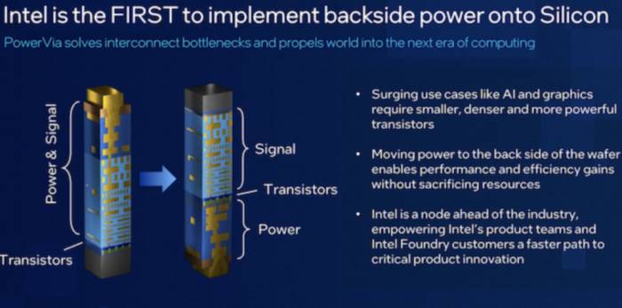
This brings us to backside power delivery. If inputting signals and power on the same side of the chip causes problems, why not separate the two? In short, this is exactly what backside power delivery aims to solve by moving all power connections to the other side of the wafer.
For Intel's PowerVia implementation of this concept, Intel actually inverts the wafer and polishes away almost all remaining silicon until they reach the bottom of the transistor layer. At that point, Intel then constructs metal layers for power delivery on the other side of the chip, similar to how they previously built them on the front side. The end result is that Intel ends up with essentially a double-sided chip, with one side transmitting power and the other sending signals.
From a theoretical standpoint (and as per Intel's papers), transitioning to BS-PDN ultimately has several benefits. Firstly, it has a significant impact on simplifying the construction of the chip. We will discuss Intel's specific claims and findings later, but it is important to note here that it allows Intel to relax the density of its M0 metal layer. The Intel 4 + PowerVia test node allows for a 36 nm pitch, instead of the 30 nm pitch required on Intel 4. This directly simplifies the most complex and expensive processing step of the entire chip, rolling it back to a size closer to the Intel 7 process.
BS-PDN is also poised to provide the chip with some modest performance improvements. Shortening the power delivery path to the transistors through a more direct approach helps offset the IR droop effect, thereby better delivering power to the transistor layer. Removing all these power lines from the signal layer can also improve their performance, eliminating power interference and providing chip designers with more space to optimize their designs.
Otherwise, the main cost of all this is the loss of the benefits of building front-end chips mentioned earlier. The transistor layer is now roughly in the middle of the chip, rather than at the end. This means that traditional debugging tools cannot directly poke through the completed chip's transistor layer for testing, and now there are about 15 layers of signal lines between the transistor layer and the cooling service. These are not insurmountable challenges, as carefully elaborated in Intel's papers, but they are issues that Intel must address in its design.
Manufacturability is another set of trade-offs involved in the transition to BS-PDN. Building power layers on the backside of the chip has never been done before, which increases the likelihood of errors. Therefore, not only does the power delivery need to work, but it also needs to work without significantly reducing chip yield or otherwise reducing chip reliability. However, if all these things are successful, the additional work of building power layers on the backside of the wafer will be offset by the time and cost saved by not having to route power through the front side.Intel's Additional Scheme: Carrier Wafer and Nano TSV
As the backside power delivery network is expected to become an industry standard feature in due course, we try not to focus too much on Intel's specific implementation of BS-PDN/PowerVia. However, now that we have understood the basics of BS-PDN, there are several Intel-specific implementation details worth noting.
Firstly, Intel is using a carrier wafer as part of its build process to provide chip rigidity. After the front side of the PowerVia wafer is manufactured, the carrier wafer is bonded to the front of that wafer. It is a virtual wafer to help support the chip while Intel is working on the other side. Since the double-sided chip manufacturing process grinds away too much of the remaining silicon wafer, there is not much structural silicon to hold the whole thing together. As Intel jokingly puts it, despite this being silicon lithography, there is only a minimal amount of silicon left on the wafer by the end.
In turn, the carrier wafer remains a part of the chip for the rest of its life cycle. Once the chip manufacturing is complete, Intel can polish the bonded carrier wafer to the required thickness. It is worth noting that since the carrier wafer is on the signal side of the chip, this means there is an additional layer of material between the transistors and the cooler. Intel's technology for improving heat transfer takes this into account, but for PC enthusiasts accustomed to mounting transistors on the top of the chip, this will be a significant change.
Another noteworthy detail of Intel's implementation of BS-PDN is the use of TSV for power wiring. In PowerVia, there are nano-scale TSVs (appropriately named Nano TSV) in the transistor layer of the chip. This contrasts with the embedded power rails that industry pioneer IMEC has been researching for its BS-PDN.
In summary, although the power rails still need to go up and over the transistor layer to deliver power, the use of TSV allows power to be delivered more directly to the transistor layer. For Intel, this is a technological advantage they are keen to leverage, as it avoids the need to design and build-in routing required for embedded power rails.
Blue Sky Creek: Intel 4 + PowerVia Test Chip
To test PowerVia and prove that it works as expected, Intel's technical verification tool is a chip they call Blue Sky Creek.
Blue Sky Creek originates from Intel's Meteor Lake platform, using two E-cores dies based on Intel Crestmont CPU architecture. There are two reasons why Intel uses Crestmont here: firstly, it was originally designed for Intel 4, making it a good candidate for porting to the Intel 4 + PowerVia process. Secondly, because E-cores are small; the size of the four-core test die is only 33.2mm² (4mm x 8.3mm), which makes a good balance between testing complexity and not having to actually produce large dies on the experimental process node.
Intel does not focus too much on the performance of the E cores in Blue Sky Creek. However, they did note that the design frequency is 3GHz at 1.1v.From a broader perspective, the existence of Big Sky Creek is part of Intel's grand plan to mitigate the risks of introducing two major technological innovations in the same process node—this issue has dealt a considerable blow to Intel's overly ambitious 10-nanometer development plan (Intel 7) process node.
As the company outlined in 2022, among these two technologies, PowerVia is considered to be the riskier of the two. For this reason, Intel will develop a temporary test node for PowerVia, enabling them to develop this technology independently of RibbonFET. Ultimately, if the development of PowerVia does not proceed as expected, Intel can still proceed with the development of RibbonFET and launch chips without PowerVia.
For similar reasons, you won't find much discussion about Intel's RibbonFET at the VLSI conference. Although this is an important technology for the company, it is essentially a foregone conclusion for Intel. The company will not even be the first foundry to adopt GAAFET technology, so while RibbonFET does indeed face its own challenges, Intel does not need to prepare any risk mitigation strategies as they do for PowerVia.
PowerVia Practice: Intel finds a 30% reduction in IR Drop
Diving into the results of Intel's PowerVia paper, the company analyzed the results of Blue Sky Creek on a per-metric basis, studying everything from chip density to performance to thermal dissipation.
Starting with chip density, here is the size of the high-performance (HP) library cells that Intel developed and manufactured for its test chips, and how these cells compare to equivalent Intel 4 cells. As previously mentioned, switching to PowerVia allowed Intel to relax the spacing of the critical M0 metal layer, expanding it from 30 nm to 36 nm. Other major parameters of the node, such as fin pitch and contact poly pitch (CPP), remain at 30 nm and 50 nm, respectively.
However, these changes, coupled with Intel's ability to reduce the number of fins in use from 3 to 2, lead to an overall smaller cell. Thanks to PowerVia, Intel was able to reduce the cell height from 240 nanometers on Intel 4 to 210 nanometers. And with CPP remaining unchanged at 50 nanometers, this means an overall cell size reduction of 12.5%, despite not using a formal "dense" node.
This disclosure also gives us a comprehensive understanding of the total number of layers involved in the two chips. A standard Intel 4 chip has 15 layers plus redistribution layers (RDL) on one side, while the PowerVia test chip has 14 layers on the signal (front) side, plus 4 additional layers plus RDL on the power (back) side. This is a net gain of 3 layers, so at least for Intel's test chips, it is more complex in terms of the total number of layers used. On the other hand, all these new layers are located on the power side of the chip, and they are all relatively large and easy to manufacture. This is why Intel believes that the additional layers are a minimal drawback compared to not having to manufacture an M0 layer with a 30 nm pitch.
The density of these cells is also quite impressive. By switching to backside power supply, Intel was able to utilize 95% of the space within a denser point in the E-core cell. Unfortunately, Intel did not provide comparable numbers for the E-core on Intel 4, but overall, the utilization rate is not as high.As for the electrical performance of the E-cores, as expected, PowerVia significantly reduced the IR drop. Compared to the E-cores embedded in Intel 4, Intel measured a 30% reduction in the drop on their test chips, and the drop at the actual chip bump level was even reduced by 80% (5 times).
This clean power delivery, in turn, improves the computing performance and energy efficiency of the chip. In addition to the direct improvement in efficiency due to the reduced energy loss due to resistance, the construction of the E-core using PowerVia technology also increased the maximum frequency (fMax) of the core by 6%. Intel did not provide a more detailed explanation of why this would increase their clock speed, but I suspect it is related to the higher voltage actually reaching the transistors themselves, allowing them to operate at a higher clock frequency.
Although a 6% increase in clock speed is not a huge gain, it is essentially a "free" improvement of a technology designed to improve chip manufacturability. In the past, Intel has been struggling to achieve smaller clock speed improvements.
Interestingly, Intel did find that the new IR drop values are not the same in all E-cores. Although the standard Intel 4 chip has a relatively consistent voltage drop across all four cores, the voltage drop on the test chip is between 60 mV and 80 mV, depending on the core. As this is a research report, Intel did not delve into the impact on their products, but assuming mass-produced chips have the same wide variability, this may mean that we will pay more attention to preferred/main cores in future products.
So PowerVia/BS-PDN can work. But can Intel mass-produce it? The answer is also yes.
According to Intel, the defect density of their experimental Intel 4 + PowerVia process node is only about one and a half times lower than the Intel 4 process itself (which is already in HVM). This means that not only is the defect density low enough for mass production in the short term, but if Intel scales this specific node to production scale, their chip yield will be similar to the current non-PowerVia Intel 4 chips, just two quarters later.
Similarly, Intel reports that the transistors built based on the PowerVia process are very similar to the transistors of the Intel 4 process. In this case, this is a good thing because it means that these transistors will not do unexpected things that affect performance or chip reliability. In this regard, Intel also pointed out that they did not observe any power-related reliability violations on the test chips, indicating that despite significant changes in power transmission, the introduction of back-end power transmission did not lead to a reduction in the reliability of the chip's power transmission system.
Although Intel did not take specific measures to mitigate the thermal impact of the transistor layer no longer being at the top of the flip-chip, the data released by the company indicates that their mitigation measures were successful.
When the thermal response curve of the Intel 4 chip is plotted, Intel's test chip shows a very similar thermal response curve. That is to say, the temperature generated at a given power level is consistent with the Intel 4 chip. As you may have noticed from Intel's chart, they even continue to overfeed the chip to simulate higher thermal loads, better characterize the thermal response curve, and ensure that thermal scaling does not break down under higher thermal densities.
As mentioned earlier, heat dissipation/cooling is one of the two major product-level challenges of back-end power supply. Placing the transistors in the middle of the chip does not bring any benefits to chip cooling, but Intel believes they have developed the necessary mitigation strategies to keep PowerVia chips consistent with traditional front-end manufactured flip-chip chips.The mitigation measures are also applicable to debugging, which is another challenge for BS-PDN. Intel has developed a set of new and modified debugging techniques to deal with the fact that both sides of the chip are now in use. At the same time, referring to the abstract of Intel's paper, "Due to the metallization on both sides of the wafer, fault debugging and defect isolation are complex," ultimately, Intel was able to develop the necessary tools.
Interestingly, Intel even placed some "Easter eggs" defects in the chip design to provide some semi-controlled defects for Intel's verification team. According to Intel, their verification team used their PowerVia debugging tool to find all these eggs, helping to prove the effectiveness of these debugging processes.
In summary, before next week's VLSI conference, Intel has made a very convincing case that their PowerVia backside power supply technology development is on the right track. In this regard, starting and running complex test chips is a big deal, because having actual data and experience to draw on is an important step towards fine-tuning the technology for mass production, while demonstrating that Intel is meeting their aggressive fab development goals so far.
Ultimately, in terms of fully regaining momentum and possibly regaining the leadership position in silicon lithography business, PowerVia may be Intel's biggest moment of success or failure. If Intel can deliver on its promises, the company is expected to be at least two years ahead of TSMC and Samsung in deploying backside power supply - which means at least two years are needed to gain the cost and performance advantages of the technology. TSMC is expected to deploy backside power supply before the N2P node at the end of 2026 or the beginning of 2027, and it is currently unclear when Samsung will make its own transition.
As for Intel, if everything continues as planned, Intel will start mass production with PowerVia in 2024, when the company plans to launch its Intel 20A and Intel 18A processes. The first consumer processor to use this technology will be Intel's Arrow Lake architecture, which will be the next generation of Core products built on the 20A node.
TSMC's backside power supply options
According to previous reports by TSMC, the company will introduce Nanosheet GAA transistors and add backside power rail technology in the N2P process to be released in 2026.
At its 2023 Technology Symposium, TSMC revealed that the backside PDN of its N2P will improve performance by 10% to 12% and reduce logic area by 10% to 15% by reducing IR Drop and improving signals. Of course, this advantage will be more obvious in high-performance CPUs and GPUs with dense power supply networks, so moving it to the back is significant for them.
Backside PDN is part of TSMC's N2P manufacturing technology, which will enter HVM at the end of 2026 or the beginning of 2027.
Regarding the implementation of PDN, TSMC did not disclose much. However, at the 2020 Technology Symposium, TSMC introduced its 3D IC packaging technology SoIC, which, according to relevant reports, is an important prerequisite for their PDN implementation. As shown in the figure, a low-temperature die-to-die bonding technology provides electrical and physical connections between dies. The following figure describes the available chip mounting options - that is, face-to-face, face-to-back, and complex combinations, including side-to-side assembly that may integrate other chip stacks.For face-to-face orientation, the backside of the top die receives signals and the PDN redistribution layer. Alternatively, a third die on top of the SoIC component can be used to implement signal and PDN redistribution layers for encapsulation bumps—later, a TSMC design test case using a three-layer stack will be described.
Silicon through-vias (TSVs) in die #2 provide electrical connections for signals and power to die #1. Dielectric vias (TDVs: through-dielectric vias) are used to encapsulate connections between the smaller die #2 and die #1 in the volume area outside of die #2.
Planning power supply to SoIC dies requires consideration of several factors:
Estimated power per die (especially when die #1 is a high-performance, high-power processing unit)
TSV/TDV current density limits
Different power domains associated with each die
The figure below highlights design options for "the number of TSVs per power/ground bump." To reduce IR Drop and observe current density limits through TSVs, a TSV array may be appropriate—e.g., the figure shows up to 8 TSVs. (Examples of FF and SS corners are shown.)
The report emphasizes that a key task in SoIC development is parallel engineering related to the allocation of bumps, pads, and TSV/TDV positions for the entire signal and PDN.
The figure above highlights a series of planning steps for developing TSV configurations for the PDN—using the face-to-face chip stacking configuration as an example. The original "virtual" pads between chips (for mechanical stability) are replaced by signal and PDN TDV and TSV arrays. (TSMC also pursues the goal of reusing probe cards between die #1 testing and final SoIC testing—this goal affects the allocation of pad and TSV positions.)
Careful selection of TSV implementation for CPU chips and SRAM chips is also required to meet IR targets without adversely affecting the overall chip interconnect density.Samsung's Backside Power Supply Scheme
According to a report by South Korean media outlet TheLec last year, Samsung is planning to develop 2nm technology using a method called Backside Power Supply Network (BSPDN).
Samsung researcher Park Byung-jae stated that in the foundry market, technology is evolving from high-k metal gate planar FETs to FinFETs, then to MBCFETs, and now to BSPDN.
FinFET, previously known as the 3D transistor, was a key chip design technology in the development of the 10nm process technology. The gate surrounds the current channel on three sides to prevent current leakage. However, the recent shift to processes below 10nm means that FinFET is no longer sufficient.
Samsung introduced the Gate-All-Around (GAA) technology that surrounds the current channel on four sides. The company added what is called nanosheets instead of nanowires and named this technology MBCFET. BSPDN is different from this and should be more understood as an evolution of the chiplet design used by Samsung, Intel, and TSMC. Chiplet is not a process applied on a single chip from one company, but rather a connection of various chips manufactured by different companies using different processes.
Also known as 3D-SoC, it also combines logic and memory. Unlike the front-end power supply network, BSPDN utilizes the back-end; the front side will have logic functions, and the back side is used for power supply or signal routing. BSPDN was first proposed as a concept at IMEC in 2019. A 2nm paper citing this technology was also presented at the 2021 IEDM.
The paper, titled "SRAM Macro and Logic Design and Optimization Using 2nm Process Back-End Interconnects" in Korean, claims that BSPDN has a 44% performance improvement and a 30% power efficiency improvement compared to FSPDN. The paper suggests that moving power supply networks and other functions to the back of the chip can solve the routing congestion problems caused by using only the front side.
Imec's View on PDN
According to imec, some chip manufacturers have publicly announced the introduction of backside power supply networks in logic ICs at the 2nm and below technology nodes. This is the time when nanosheet transistors are making progress. However, novel routing technology can be used for a wide range of transistor architectures. Imec's roadmap foresees its introduction in advanced technology nodes, as well as nanosheet transistors in 6T standard cells. The combination with BPR will help push the standard cell height below 6T.
But the application field is not limited to 2D single-chip ICs: it is also expected to improve the performance of 3D system-on-chips (3D SOC). Imagine a 3D-SOC implementation where some or all memory macros are placed in the top die, and logic is placed in the bottom die. In terms of technology, this can be achieved by bonding the active front of the "logic wafer" to the active front of the "memory wafer". In this configuration, the original back sides of the two wafers are now on the outside of the 3D-SOC system. We can now consider using the "free" back of the "logic wafer" to power the power-hungry core logic circuits. This can be done in the same way as proposed for 2D SOCs. The main difference is: the original dummy cover wafer - introduced before to make the wafer thinner - is now replaced by a second active wafer (in this case, the memory wafer).Although this design has not yet been implemented through experiments, the preliminary evaluation from the perspective of IR voltage drop is very encouraging. The proposed solution has been verified on the memory partition design in logic using the Advanced Node Process Design Kit (PDK). The implementation of the backside power supply network using nTSV and BPR has shown promising results: the average and peak IR voltage drop at the bottom die were reduced by 81% and 77% compared to the traditional front-side power supply. This makes the backside power supply an ideal choice for 3D IC power supply in advanced CMOS nodes.
For 2D and 3D designs, the concept of utilizing the backside of the wafer can be extended to other functions by adding specific devices (such as I/O or ESD devices) on the backside. For example, Imec combines backside processing with the implementation of 2.5D (i.e., pillar) metal-insulator-metal capacitors (MIMCAPs) as decoupling capacitors. The 2.5D MIMCAP increases the capacitance density by 4 to 5 times, thereby further improving the IR voltage drop. The results stem from an IR voltage drop modeling framework calibrated with experimental data.
In Imec's view, future chips are likely to break away from the tradition of front-side power supply. The backside power supply network with backside metal, embedded power rails, and nTSVs shows clear advantages in reducing IR voltage drop, relieving BEOL wiring pressure, and improving standard cell height scaling. Key process steps such as BPR integration, wafer bonding, wafer thinning, and nTSV processes are gradually being perfected, preparing for the introduction of advanced logic technology nodes and future 3D SOCs with new wiring technologies.
Leave A Comment