A 15.3 billion transistor chip was released, AMD officially challenged NVIDIA.
Driven by the wave of generative AI, AMD has also become a winner in the semiconductor market.
According to the latest data, since the beginning of this year, AMD's market value has soared by more than 90%. If we extend the timeline to five years, AMD's market value has soared by more than 660%. Behind this, in addition to the generative AI mentioned at the beginning of the article, AMD's push for CPU products based on the ZEN architecture and CDNA architecture products specifically designed for data center dedicated GPUs, the acquisition of Xilinx and Pensando's FPGA and DPU, as well as the company's investment in technologies such as Chiplet and 3D V-Cache, have made significant contributions.
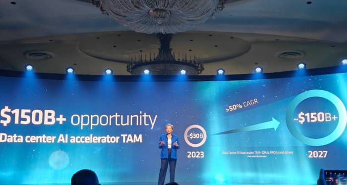
At today's product launch in San Francisco, AMD CEO Lisa Su even said, "We are still in a very, very early stage of the AI life cycle." According to their estimates, the TAM for data center AI accelerators will reach $150 billion by 2027, which means that the CAGR for the next four years will exceed 50%.
It is precisely under the drive of such a huge market demand that AMD has brought more details and updates to the company's latest and highly competitive AMD Instinct MI300 series products. At the same time, AMD also brought updates to the fourth generation of Epyc products, fully embracing the new era of data centers.
Advertisement
The 153 billion transistor monster chip makes a shocking debut
At AMD's launch today, the most eye-catching product is undoubtedly the company's Instinct MI 300 series. Because in the AI era dominated by Nvidia GPUs, everyone hopes that AMD's series of chips can become the strongest competitor to the trillion chip giant. From the parameters provided by Lisa, the new chips of the MI 300 series have very strong competitiveness.
"Artificial intelligence is the decisive technology shaping the next generation of computing and is also AMD's largest strategic growth opportunity," Lisa Su emphasized.
Readers who are familiar with AMD should know that the MI 300 is an important product they launched in June last year, targeting AI and HPC. By integrating CPUs and GPUs into a chip in the form of chiplets and adopting a unified memory architecture, AMD hopes that this market can bring different products to the AI market.Today, AMD has introduced the AMD Instinct MI 300X, an accelerator specifically designed for generative AI. Unlike the AMD Instinct MI 300A, the AMD Instinct MI 300X does not integrate CPU cores but instead features a design with 8 GPU chiplets (based on the CDNA 3 architecture) and an additional 4 IO memory chiplets. This results in an astonishing 153 billion transistors integrated into the chip. To alleviate the memory constraints faced by large AI language models (LLMs), AMD has integrated 192GB of HBM 3 into this chip, with a storage bandwidth of up to 5.2 TB/s, capable of handling up to 40 billion parameters.
As a product that competes with NVIDIA's H100, as shown in the figure, the HMB density of the AMD Instinct MI 300X is 2.4 times that of the former, and the bandwidth is 1.6 times that of the former. This greatly enhances the competitiveness of AMD's product in the current AI era. At the same time, according to AMD, based on the AMD Infinity architecture with a bandwidth of up to 896GB/s, we can combine eight M1300X accelerators in a system, providing more powerful computing capabilities for development and offering different solutions for AI inference and training. AMD has introduced that the chip will be sent for sampling in the third quarter of this year. It is worth mentioning that this design method is also the choice for NVIDIA's 8-way HGX and Intel's Ponte Vecchio X8 UBB.
As mentioned earlier, AMD also launched the AMD Instinct MI300A at the same time, which is the world's first APU for AI and HPC, featuring an integrated design with 24 Zen 4 cores, CDNA3 GPU cores, and 128GB HBM3. In other words, unlike MI 300X, which only integrates GPU cores, the AMD Instinct MI300A integrates both CPU and GPU in its design. Compared to MI250, this product offers 8 times the performance and 5 times the efficiency. In the previous article "AMD's Largest Chip: 13 Chiplets, 146 Billion Transistors" by Semiconductor Industry Observation, we introduced this first-generation product.
According to foreign media semianalysis, MI300A has made headlines with its heterogeneous CPU+GPU computing, and the El Capitan Exascale supercomputer is using this version. They pointed out that MI300A uses an integrated heat sink packaging design on a 72 x 75.4mm substrate, suitable for the SH5 LGA motherboard slot, with 4 processors per board, effectively paying for development costs. Semianalysis revealed that the chip has been shipped, but there will be a real increase in the third quarter, which is consistent with AMD's statement. They further pointed out that the standard server/node will be 4 MI300As. There is no need for a host CPU because it is built-in.
"This is the best HPC chip on the market to date and will remain so for some time," semianalysis emphasized.
While releasing these AI application chips, we naturally cannot avoid AMD's investment in software, which many analysts believe will be a weakness for AMD in this market. However, from the introduction by AMD President Victor Peng, we can see that they have also set a goal in this market, that is, Open (software approach), Proven (AI capability), and Ready (support for AI models).According to Victor Peng, AMD has a complete set of libraries and tools called ROCm that can be used for its optimized AI software stack. Unlike proprietary CUDA, this is an open platform. In the past development, the company has been continuously optimizing the ROCm suite. AMD is also collaborating with many partners, hoping to further improve its software to facilitate developers' AI development and application.
"We have made real great progress in building a powerful software stack that can work in conjunction with an open ecosystem of models, libraries, frameworks, and tools," said Victor Peng.
The much-anticipated Bergamo has arrived as scheduled.
While introducing the MI300, AMD also introduced another major product of the company today - the new generation of EPYC. This is a series of chips designed for data centers. In the fourth generation, AMD has prepared four product lines targeting different markets, including the much-anticipated Bergamo series, which is designed for cloud-native computing needs, and the second-generation EPYC 3D V-Cache CPU with the codename Genoa-X.
According to Lisa Su, the new generation of AMD EPYC Genoa has a performance in cloud workloads that is 1.8 times that of Intel's competitive processors, and the speed in enterprise workloads is 1.9 times that of Intel's competitive processors. Lisa also mentioned that most artificial intelligence runs on CPUs, and AMD's products have an absolute performance advantage over competitors' Xeon 8490H in this aspect, with a performance that is 1.9 times higher and efficiency that is also 1.8 times that of competitors.
After introducing EPYC Genoa, Lisa focused on introducing the company's cloud-native product Bergamo, a high-density server CPU that developers have been looking forward to for a long time. According to the introduction, the chip is based on AMD's density-optimized Zen 4c architecture, providing up to 128 CPU cores, which is 32 more cores than AMD's current flagship EPYC 9004 "Genoa" chip. In the view of AMD CTO Mark Papermaster, Zen 4c is a complement to AMD's compact density and a new track on the company's core roadmap, providing the same functionality as Zen 4 in about half of the core area.In the view of analysts, the purpose of the Zen 4c and Bergamo design is to provide as many computing resources as possible. This is a decision made by AMD to continue to increase the demand for core numbers to meet customer needs in the face of the failure of Moore's Law. According to data provided by AMD, the brand new Zen 4C core can reduce the area by 35%, and the number of cores that can be provided in each CCD is twice that of Zen 4, and it can increase the core by 33% in each Socket. In other words, each CCD of Zen 4 has 8 cores, while each CCD of Zen 4c has 16 cores. This also means that the total number of CCDs in the Zen 4c EPYC chip is less than its original Zen 4 chip.
According to AMD, the Bergamo released this time only uses eight Zen 4C Chiplets and a central IO Chiplet, which is slightly different from the standard EPYC chip that can use up to twelve Zen 4 Chiplets. Thanks to this design, Bergamo has become a design with 8.2 billion transistors, which is lower than the about 9 billion transistors in the complete Genoa chip. This higher core number and smaller clock speed design make the chip more energy-efficient than the Genoa design - this is an important factor considered by AMD when defining the market for this product. AMD also revealed that Bergamo's performance and efficiency are also very outstanding.
Relying on its high core density and high energy efficiency, AMD hopes that Bergamo can compete with Ampere, Amazon, and other companies that use Arm architecture cores in this field, and AMD also hopes that this chip will become a strong competitor to the 144-core Sierra Forest that Intel will launch in 2024.
In addition to the above products, AMD has also brought the "Genoa-X" EPYC processor with 1.1GB L3 cache. It is understood that Genoa-X is the successor to AMD's first generation V-cache Milan-X. Like the previous generation, AMD is using cache chip stacking to add more L3 cache to other regular Genoa Zen 4 CCDs. Under this design, there are 12 CCDs on the Genoa/Genoa-X chip, which allows AMD to add an additional 768MB of L3 cache to the chip.
More chips are on the way.
At this event, AMD also disclosed a brand new DPU plan, which is the technology they obtained through the acquisition of Pensando. In their view, AMD's Pensando SmartNIC is an indispensable part of the new data center architecture. According to AMD's plan, they will integrate the P4 DPU offload into the network switch next, providing services at the rack level. To this end, they are developing an intelligent switch with HPE Aruba Networks.
AMD also emphasized its next-generation DPU roadmap codenamed "Giglio", which aims to bring higher performance and energy efficiency to customers compared to the current generation of products, and is expected to be launched at the end of 2023. AMD also released the AMD Pensando Software-in-Silicon Developer Kit (SSDK), enabling customers to quickly develop or migrate services for deployment on the AMD Pensando P4 programmable DPU, in coordination with the existing rich feature set of the AMD Pensando platform. The AMD Pensando SSDK enables customers to leverage the powerful capabilities of the leading AMD Pensando DPU, and customize network virtualization and security functions in their infrastructure, in coordination with the existing rich feature set implemented on the Pensando platform.Relying on these rich products, AMD is striving to reach the next peak in the data center.
Leave A Comment