What to pay attention to in advanced packaging?
Despite the overall economic downturn, the advanced packaging market continues to show resilience.
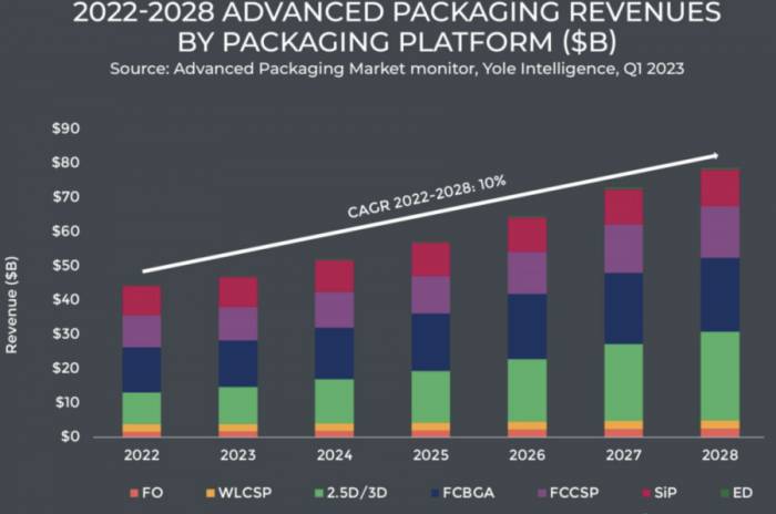
According to the latest report from Yole Group, revenue in 2022 grew by about 10% compared to the previous year. The market was valued at $44.3 billion in 2022 and is expected to have a compound annual growth rate (CAGR) of 10.6% from 2022 to 2028, reaching $78.6 billion by 2028.
The report further points out that high-performance packaging for integrating chips with more advanced nodes is expected to exceed $16 billion by 2028, accounting for more than 20% of the advanced packaging sector. Among the different advanced packaging platforms, 2.5D/3D is growing the fastest, with a CAGR close to 40% from 2022 to 2028. It is one of the most analyzed and developed technologies, with a significant share of revenue.
At the recent Electronic Components and Technology Conference (ECTC), Yole's analysts shared some insights into the future development of advanced packaging.
Chiplets and Heterogeneous Integration Revolutionize Advanced Packaging
In Yole's view, as Moore's Law slows down and the complexity and cost of cutting-edge nodes increase, advanced packaging is becoming a key solution for integrating multiple dies into a single package, potentially combining mature and advanced nodes. Heterogeneous integration and chiplet-based methods have become essential in segments such as artificial intelligence, networking, autonomous driving, high-end PCs, and high-end gaming. Heterogeneous integration enabled by advanced packaging technology can achieve cost-effective multi-chip integration in a compact plane and also provide superior performance compared to traditional packaging.
Advertisement
Integrating a larger number of active circuits within the package is a method of assigning different functions to different chips integrated into the same package through dense interconnections. The time to market is also shortened, as chips can come from different manufacturers and be assembled.
Octopart revealed in an article that to manufacture chiplet-based products, you need design skills, dies, connections between the dies, and production strategies. The performance, price, and maturity of chiplet packaging technology have a substantial impact on the application of chiplets. Depending on the connection medium and method, packaging technology for chiplet interconnection can be divided into three categories: substrate packaging, silicon-interposer packaging, redistribution-layer (RDL) packaging, and embedded multi-die interconnect bridge (EMIB).
Let's first look at substrate packaging. The popular choice for substrates is organic materials because they are readily available. Similar to traditional PCBs, wiring connections are made through an etching process that is independent of other processes used in semiconductor manufacturing. This is the earliest incarnation of the most well-known 2D heterogeneous integration.
Multiple dies can be easily connected to the substrate at high density through flip-chip design or stacking. In addition, the associated material and manufacturing costs are extremely low because this technology does not rely on chip manufacturing processes. The main disadvantage of using this technology is the low I/O pin density, which limits the bandwidth of interconnections in these packages.Next, consider the silicon interposer packaging, which covers 2.5D and 3D packaging technologies. The chips are built laterally on the interposer layer (2.5D) or stacked vertically (3D). To achieve interconnects and communication between the dice, the silicon interposer is placed between the substrate and the dice. The interposer acts like a miniature printed circuit board, essentially providing a substrate for the electrical connections between the small chips. The interconnect structure consists of metal bumps (called microbumps) and through-silicon vias (TSVs) that run inside the package. These are used to connect the dice to the interposer and the interposer connectors to the package substrate with a BGA pad pattern.
These products have higher I/O density, lower power consumption, and lower transmission latency. This is achieved through shorter wiring lengths and spacings between the microbumps and TSVs. The only significant drawback of this technology is the increased manufacturing cost.
Looking again at the RDL packaging technology, the Redistribution Layer (RDL) packaging technology does not use a substrate, but instead, dielectrics and metals are directly deposited on the top surface of the wafer. This technology is also known as "fan-out" technology. To carry the wiring design, a redistribution layer is constructed, allowing each small Chiplet's I/O ports to be shaped around the device. By shortening the length of the circuits, RDL provides higher signal integrity (lower loss and distortion).
As for EMIB, it is a technology that uses a thin silicon wafer part embedded in an organic material as a chip-to-chip interconnect substrate. The issue of higher costs for high-end products can be resolved by using a bridge packaging with different Chiplets. This hybrid packaging technology is a combination of substrate-based and interposer-based packaging. Thin silicon layers, typically less than 75 micrometers, are coated on the substrate and used to form chip-to-chip connections, with these layers embedded in the organic substrate layer.
The concept follows the same idea as ELIC in HDI PCBs, where each interconnect structure connects multiple chips to the inner layer of the insulating (organic) substrate. The EMIB part of the package is a silicon bridge that provides high-bandwidth connections between small chips.
Hybrid bonding is everywhere
Yole emphasizes in the article that several sessions at ECTC are dedicated to discussing hybrid bonding. In their view, this technology is becoming the key to heterogeneous integration and progress in assembly technology within the chiplet space, as it allows for high-density vertical stacking of different chips within the package.
Hybrid bonding can be wafer-to-wafer, die-to-wafer, or die-to-die. Its main advantage is that it allows for 3D device stacking for vertical scaling and higher interconnect density than other chip stacking technologies. Another feature is that fine-pitch bonding leads to higher interconnect density. This also increases system bandwidth and power efficiency. Speed is also improved, as traditional bumps are eliminated, and direct copper-to-copper bonding is used instead. This forms very tight interconnects and, as the pads are part of the chip structure, improves bonding strength and reliability.
According to BrewerScience, hybrid bonding is the key to pioneering the future of advanced packaging innovation. Because hybrid bonding provides a solution that can achieve higher bandwidth as well as higher power and signal integrity. As the industry is looking to improve the performance of the final device by extending system-level interconnects, hybrid bonding offers the most promising solution, capable of integrating multiple dice with small interconnect spacing less than 10 µm.
And to understand the basics of hybrid bonding, three fundamental questions need to be asked: What is hybrid bonding, why use hybrid bonding, and which materials are most suitable for your application?BrewerScience states that as the electronic packaging industry evolves to three-dimensional (3D) packaging, microbumps provide vertical interconnections between chips by utilizing small copper bumps on the wafer as a form of wafer-level packaging. The size of the bumps ranges from 40 µm pitch to eventually shrinking down to 20 µm or 10 µm pitch. However, this is where the challenge lies; scaling down beyond 10 µm becomes very challenging, and engineers are turning to a new solution to continue scaling down. Hybrid bonding offers a solution for 10 µm and below spacing by completely avoiding the use of bumps, instead using small copper-to-copper connections to connect the dies in the package. It provides superior interconnect density, supporting 3D-like packaging and advanced memory cubes.
"Hybrid bonding is a permanent bonding that combines dielectric bonding (SiOx) with embedded metal (Cu) to form interconnects. It is known throughout the industry as Direct Bond Interconnect (DBI). Hybrid bonding extends fusion bonding, which embeds metal pads in the bonding interface, allowing face-to-face connection of wafers," emphasizes BrewerScience.
This is because hybrid bonding vertically connects the dies to the wafer (D2W) or wafer to wafer (W2W) through closely spaced copper pads. While W2W hybrid bonding has been in production in the imaging sensor field for many years, the industry is still vigorously promoting the development of D2W hybrid bonding. This development will further enable heterogeneous integration, providing a powerful and flexible way to directly connect chips with different functions, sizes, and design rules.
Compared to other bonding technologies, hybrid bonding has many advantages, including: allowing advanced 3D device stacking, the highest I/O achieving bonding spacing below 10 µm, higher memory density, expanded bandwidth, increased power, improved speed efficiency, eliminating the need for bumps, and enhancing performance without power and signal loss.
However, some speakers at ECTC discussed improvements that can be made in the development of hybrid bonding technology, such as increasing bonding strength. There is also room for improvement in yield. Contamination issues can also affect hybrid bonding; although the risk of contamination is not higher than other technologies, the impact of particles blocking propagation is greater due to the small spacing.
Glass, emerging as a new choice for packaging materials
In addition to new technologies, ECTC also discussed new materials. Among them, glass is becoming one of the key materials available for packaging. It has many advantages, such as high thermal conductivity, mechanical strength, low dielectric constant, and low dielectric loss. It can also create fine lines and spaces, allowing for small spacing, and its CTE (coefficient of thermal expansion) is closer to silicon than other organic materials commonly used for packaging.
This material has also become popular in RF, HPC, photonics, and CPO (co-packaged optics) applications.
ECTC participants saw developments around glass substrates and glass interlayers, including close collaboration between Georgia Tech and glass suppliers and IC substrate suppliers to develop reliable and high-performance solutions. One area under development is glass core substrates to replace the organic core of traditional IC substrates. This is mainly applicable to HPC and RF applications.
In addition to being more cost-effective compared to silicon, glass has many advantages. It allows for the integration of chips into large packages while providing better planarity, which is crucial for HPC and AI applications. Its low dielectric constant will be critical when frequencies exceed 5G, and 6G and 7G will further increase frequencies.The challenges of building IC substrates with glass cores and using glass to replace silicon interposers are related to the weight of the glass and the CTE (Coefficient of Thermal Expansion) differences between the glass surrounding the core and the organic layers, which could affect the reliability of the packaging. Another issue is that the metallization process for building traces is more difficult with glass than with silicon. However, this is a relatively minor issue and is likely to be resolved.
Japanese material supplier Hoya, as well as American companies Corning and Schott, are interested in entering this field.
According to a paper titled "Leveraging Glass Properties for Advanced Packaging," glass offers many opportunities for advanced packaging. The most obvious advantage is the material properties. As an insulator, glass has low electrical loss, especially at high frequencies. The relatively high rigidity and the ability to adjust the thermal expansion coefficient provide advantages for managing warpage in the bonded stacks of glass core substrates and glass through vias (TGV) and carrier applications. Glass also offers advantages for developing cost-effective solutions. Glass forming processes have the potential to form panel formats and thicknesses as low as 100 microns, providing opportunities to optimize or eliminate current manufacturing methods.
Glass has many properties that make it an exciting material for various packaging applications. Compared to silicon, the electrical performance of glass reduces electrical loss. This becomes even more important at high frequencies, which is the path that next-generation mobile technology may adopt. The significance lies in the ability to increase the functionality of smartphones while maintaining battery life.
Adjusting material properties, such as CTE, greatly facilitates the use of glass as a TGV substrate for various forms of 2.5D and 3D applications. In addition, the ability to form high-quality glass plates that are thin and large provides many opportunities for cost-effective implementation. Processing technologies that demonstrate effective processing of ultra-thin glass are being showcased.
The formation of well-formed vias and blind holes has been proven, and excellent Cu filling performance in glass in wafer and panel formats can be achieved using existing metallization technologies. The reliability of Cu-filled vias in glass has been demonstrated. These developments make glass an exciting material for next-generation packaging applications.
However, so far, there has been no mass production, and the integration of glass in packaging is unlikely in the coming years, as some ongoing challenges still need to be addressed. However, it is reported that glass substrate supplier Absolics is expected to start small-scale production of glass core IC substrates later this year or early in 2024.
Co-Packaged Optics (CPO) is becoming a reality.
According to Yole, another trend in the packaging field that is gaining attention is CPO, which is related to the networking and data center markets, where the demand for increased bandwidth is driving the development of photonic interconnects to improve speed and reduce power consumption.
CPO involves packaging electronic components and photonic chips, such as ASICs or CMOS chips interconnected with photonic chips. In this field, companies have collaborated: there were presentations at ECTC from networking and data center, chip suppliers, foundries, OSATs, R&D institutions, and material suppliers. Many are focusing on advanced substrates, where interconnections between two chips are achieved through IC substrates.Yole stated that over the past 50 years, mobile technology innovation has been introduced every decade. The demand for mobile bandwidth has evolved from voice calls and text messages to ultra-high definition (UHD) video and various augmented reality/virtual reality (AR/VR) applications. Despite the profound impact of the COVID-19 outbreak on the supply chain of telecommunications infrastructure, global consumers and enterprise users continue to create new demands for network and cloud services. Social networks, business meetings, UHD video streaming, e-commerce, and gaming applications will continue to drive growth.
The average number of devices connected to the internet per household and per capita is increasing. With the emergence of new digital devices with higher functionality and intelligence, Yole observes a higher adoption rate every year. In addition, the expansion of machine-to-machine applications such as smart meters, video surveillance, healthcare monitoring, connected drives, and automated logistics has significantly promoted the growth of devices and connections, and driven the expansion of data center infrastructure.
The co-packaged optics (CPO) community faces a difficult period due to budget cuts, as pluggable devices have already achieved the cost savings and low power consumption promised by CPO. Full deployment of CPO will only occur when pluggable functionality is exhausted. At least for the next two generations of switch systems, it is difficult to compete with pluggable modules, which will remain the preferred choice for a long time. CPO has recently attracted widespread attention for its network energy efficiency in data centers (DC). Yole's analysis shows that the power saved by the network is negligible compared to the total power consumption of the DC. Only Broadcom, Intel, Marvell, and a few other CPO participants will bring proprietary solutions to the market. To meet market demand and convince end-users of the feasibility of CPO,
With the arrival of 6.4T optical modules, fierce competition between CPO and pluggable optics may occur in 2029. At that time, multiple technical obstacles in CPO systems are expected to be resolved. However, the transceiver industry is continuously committed to innovation to promote the pluggable optics market. Before CPO systems achieve mass shipments in network applications, pluggable will adopt a co-packaged approach, and the optical engine will gain more popularity in high-performance computing and future disaggregate systems. The industrial ecosystem surrounding machine learning (ML) system vendors Nvidia and HPE, including Ayar Labs, Intel, Ranovus, Lightmatter, AMD, GlobalFoundries, and others, has made good progress and plans to achieve mass shipments of products between 2024 and 2026.
Yole predicts that 800G and 1.6T pluggable modules will be popular because they utilize 100G and 200G per-wavelength optical devices, thus they can be implemented in a technically and cost-effective manner in QSFP-DD and OSFP-XD form factors. In terms of the required electrical and optical density, thermal management, and energy efficiency, the pluggable form factor's ability to support 6.4T and 12.8 capacity will be limited. Due to the use of discrete electrical devices, power consumption and thermal management are becoming limiting factors for future pluggable optical devices. Co-packaging using a silicon photonics technology platform aims to overcome the above challenges.
Yole further points out that today, the supply chain of the pluggable optical module market is well-established. It includes suppliers of discrete or integrated components, optical companies that produce transmitter and receiver optical sub-assemblies (TOSA and ROSA), multiplexers, digital signal processors (DSP) and PCBs, as well as assembly/test integrators. In such a multi-supplier market model, there are many different suppliers involved. In addition, the interoperability of multiple different pluggable modules in a switch box helps the industry's flexibility. These are the main advantages over CPO, which will heavily rely on silicon photonics. With highly integrated optics and silicon chips, new engineering capabilities and foundries will be very much needed, which is unacceptable for traditional medium-sized enterprises.
However, Yole also frankly stated that although the mainstream deployment of high-end CPO solutions is mainly aimed at large cloud operators, there are still a large number of smaller enterprise data centers that have not yet adopted the latest interconnect technology, so the technology exchange is slower. This means that even if CPO becomes mainstream technology, pluggable modules will still be in high demand in several applications where CPO is technically or economically unfeasible, such as long-haul applications and edge data centers. For this reason, Yole predicts that pluggable technology will not be eliminated in the next 10 years. However, the pluggable optics industry may consolidate, and the CPO market will form a multi-supplier business model.
Future Efforts and Challenges
According to Yole, at the ECTC, there were also discussions about some introductions involving fan-out packaging methods, while others studied glass substrates. In addition, various interconnect technologies were discussed. Microbumps, TSV, RDL, silicon bridges, and silicon interposers are all experiencing technical improvements.
Yole reiterated that in the past few years, the semiconductor supply chain has been hit by situations such as Covid-19, chip and material shortages. This has caused disruptions in various aspects and has begun to prompt local governments to invest in domestic semiconductor production.At ECTC, they discussed the efforts of the CHIPS Act to introduce advanced packaging to North America. A strong collaboration and partnership between different elements of the domestic supply chain were observed, including design, equipment manufacturers, material and equipment suppliers, R&D institutions, and even OSATs.
In addition to carrying out more advanced packaging R&D activities in the United States, one of the goals is to support the transition from R&D to manufacturing and commercialization, but companies unanimously agree that there is a need for more cleanroom space, which requires infrastructure investment. This also takes time. In the United States, high labor costs, skill shortages, and funding requirements still hinder the development of the domestic supply chain. The same factors apply in Europe.
The heterogenous integration supported by advanced packaging is driven by the fact that the cost and difficulty of producing advanced front-end nodes today are higher. Historically, packaging has been an OSAT business, and they are still very important in this field. However, TSMC and IDMs (such as Samsung and Intel) have proposed advanced backend solutions in the past decade and have used their front-end capabilities to achieve 2.5D or 3D solutions, such as silicon interposers, silicon bridges, and hybrid bonding.
The performance level required by system requirements to meet the growing demands of digitalization, the rise of AI, and networks, 5G, and autonomous driving cannot be met solely by reducing silicon nodes due to the associated costs and yield losses. Therefore, attention is focused on advanced packaging to integrate chips from advanced or mature nodes to reduce system costs.
Advanced packaging, especially high-end performance packaging, will rely on overcoming challenges in placing multiple dies in the same package, increasing the spacing between dies, interconnect density, and bandwidth. Therefore, the industry is seeking heterogenous integration and hybrid bonding, while also researching new materials with cost-effectiveness and improved performance, as well as new technologies such as CPO, to elevate advanced packaging to a new level to meet the performance requirements of the next generation.
Leave A Comment