Moore's Law slows down, how does Multi-die lead chip innovation?
Over the past 50 years, the semiconductor industry has been advancing in line with Moore's Law, with the density of transistors continuously increasing to the level of billions, bringing about significant challenges in terms of density and cost. As Moore's Law approaches its limits, traditional monolithic semiconductor devices can no longer meet the performance or functional requirements of some compute-intensive, heavy workload applications. How to further effectively improve chip performance while keeping costs within a range that design companies can afford has become a common challenge in the semiconductor industry chain.
In response, Synopsys has proposed a new design concept—"SysMoore." "Sys" comes from System, referring to the need to enhance chip performance at the system level, not just by integrating more transistors on the wafer. In the era of SysMoore, Multi-Die systems are becoming a solution to surpass Moore's Law and address the challenges of system complexity. They can achieve the expansion of system functions more quickly and economically, reduce risks, shorten product time to market, achieve higher throughput with lower power consumption, and quickly create new product categories. And Gordon Moore himself predicted, "It may prove more economical to build large systems by packaging and interconnecting smaller, separately packaged functions."
Advertisement
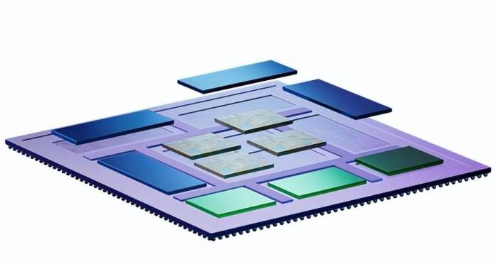
Multi-Die is becoming a major trend in industry development.
The Multi-Die system, which places multiple dies (or small chips) under one package, has many advantages:
- Accelerate the expansion of system functions at a cost-effective price (>2X reticle limits)
- Reduce risk and time to market by reusing verified designs/dies
- Improve throughput by up to 30% while reducing system power consumption
- Quickly create new product variants for flexible portfolio management
Which markets are more likely to adopt Multi-Die systems? According to Synopsys' survey of designs using Multi-Die systems, in terms of application fields, servers/AI dominate, network cards/switches are also commonly used, and the adoption in the smartphone/graphics/PC field is mainly some specialized chips, followed by some optoelectronic co-packaged and automotive fields that are moving towards Multi-Die; in terms of process nodes, the proportion of Multi-Die adoption in the 5nm process is the largest, followed by 7nm and 3nm.With the advancement of advanced packaging technologies such as 2.5D and 3D, the implementation of Multi-Die systems is becoming increasingly possible. There are already several commercial examples of Multi-Die in the industry. Not only are traditional chip manufacturers developing towards Multi-Die, but hyperscale data center manufacturers, autonomous driving car manufacturers, network companies, and others are also designing their own chips and promoting the transformation of the Multi-Die architecture in various ways, such as AMD's 3D V-Cache, Apple's M2, Intel's Meteor Lake processor, Sony's CIS, Lightmatter, Tesla, etc. These manufacturers have special requirements for performance, security, and reliability, and Multi-Die can meet their needs in specific fields.
However, the migration from a monolithic SoC to a Multi-Die system is not an easy task. The transition from a monolithic SoC to a Multi-Die system brings unique challenges that must be addressed holistically: for example, heterogeneous system integration, power consumption and thermal management, system design planning, Die-to-Die connections, software development and modeling, system verification capabilities/performance, system sign-off analysis, hierarchical testing and repair, reliability and security, system yield, memory utilization and consistency, and so on. When making every choice and decision, all aspects and their impact on the overall PPA (Power, Performance, and Area) goals of the design should be considered.
So at this point, the intervention of EDA and IP products is needed to help customers from system planning to implementation and joint development of firmware/hardware/software, to better realize Multi-Die systems.
How to build a Multi-Die system?
So, to design a Multi-Die system, what are the important steps and considerations from the overall system perspective?
Firstly, at the beginning of the design, that is, in the early architectural exploration stage, an analytical approach must be adopted to consider various macro-architectural decisions, such as IP selection, hardware/software decomposition, system-level power consumption analysis, and interconnection/storage size annotation. In addition, Multi-Die macro-architectural decisions related to aggregation (using multiple bare chips to assemble a system) and decomposition (dividing the application to multiple bare chips) must also be considered.
Early architectural decisions made around several key areas can improve the design process in the following ways: first, the system is divided into multiple bare chips, and it is necessary to meet the needs of expansion, manufacturing, and functionality; second, it is necessary to optimize the Multi-Die system, including optimizing bandwidth density, energy per bit, cost, and latency, choosing the chip's protocol and interface, such as UCIe, etc.; finally, using Multi-Die system models to assess the impact of different manufacturing and packaging technologies on performance, and accelerating the implementation of the architecture.
After the architectural exploration is completed, another major challenge is the issue of heat dissipation. Multi-Die systems integrate multiple components, and the dense transistor density generates a large amount of heat. Especially in the architectural design of Multi-Die systems, there is almost no space for heat dissipation. If the heat cannot be dissipated, the chip's functionality may be affected by mechanical stress or warping. Therefore, thermal analysis is required to conduct power analysis, power integrity, electro-thermal simulation, and mechanical analysis of the entire system to meet the key performance indicators of power consumption and heat dissipation.Additionally, a very important point is that Multi-Die systems also require a unified approach for the collaborative design of dies and packaging, including design, analysis, and signoff, to accelerate the design closure loop of these systems. At the same time, considering the complexity of the software running on such complex systems, it is essential to start the verification process as early as possible, hence the need to create virtual prototypes of multi-mode systems to support software development. Multi-Die system software development and system verification require some key considerations and solutions. Multi-abstract system modeling can leverage fast, scalable execution platforms that use virtual prototypes, simulation, hybrid simulation, and prototyping. Generally speaking, 30 billion gates are the best expansion systems for Multi-Die. By using verified models, processing procedures, and speed adapters, the software verification cycle is optimized, including die-to-die interface verification and Multi-Die system verification, to minimize startup time.
It is worth mentioning that the automation in the current tool flow has improved the efficiency of architectural exploration, surpassing the manual predictions based on spreadsheets in the past few years. Looking ahead, unified design space exploration will further improve the accuracy and efficiency of this process.
Synopsys's Comprehensive Multi-Die System Solution
It can be seen that the implementation of Multi-Die systems requires an understanding of the interdependencies between all the aforementioned design processes. In this regard, Synopsys provides a comprehensive and scalable Multi-Die solution in the industry, providing a faster path to the successful implementation of Multi-Die. This solution includes a comprehensive set of EDA tools and IPs, not only supporting early architectural exploration, rapid software development and verification, efficient die/package co-design, and robust and secure die-to-die connections, but also improving chip health and reliability. The design engine that has been tested in production, along with golden signoff and verification technology, can minimize risks and accelerate the creation of outstanding systems.
Specifically, in terms of early architectural exploration, Synopsys's Platform Architect® provides architects and system designers with a tool and efficient method based on SystemC® transaction-level model (TLM) for early analysis and optimization of the performance and power consumption of multi-core SoC architectures. Platform Architect enables system designers to explore and optimize the hardware-software partitioning and configuration of SoC infrastructure, especially the global interconnect and memory subsystem, to achieve the appropriate system performance, power consumption, and cost.
In terms of software development, Synopsys's Virtualizer can accelerate the development and deployment of Multi-Die system virtual prototypes, and the Virtualizer solution can provide higher productivity, allowing developers to obtain high-quality software at the fastest speed (as shown in Figure 7). In terms of system verification simulation, Synopsys's ZeBu and HAPS can be used for complex software and system verification (Figure 8). Among them, Synopsys ZeBu®EP1 is the industry's first unified simulation and prototyping system, which allows users to utilize this single verification hardware system throughout the chip development lifecycle. HAPS-100 allows designers, software developers, and verification engineers to manage multi-design, multi-user deployments through the HAPS Gateway to achieve maximum productivity and cost efficiency.In the implementation of Multi-Die system design, Synopsys' 3DIC Compiler platform is a comprehensive end-to-end solution. It integrates many transformative Multi-Die design functions, providing a complete platform from architecture to signoff. This enables efficient 2.5D and 3D Multi-Die system integration. The internal golden signoff tools ensure that each parameter can be accurately, completely, and conveniently signoff.
In addition to this, Synopsys can also provide a series of reliable and secure IPs that have been silicon-verified, including UCIe for high-bandwidth, low-latency die-to-die connections, HBM for high-bandwidth, low-power memory, and secure interfaces for preventing tampering and physical attacks, etc.
To ensure the final yield and reliability of the product, it is necessary to test the product quality, including comprehensive testing, debugging, and repair of each die, memory, interconnection, and the entire system in the Multi-Die system. Especially, a multi-system design like 3DIC poses unique testing challenges, and IEEE Std 1838-2019 is a standard that 3DIC must meet. Ultimately, it ensures the availability of known good dies (KGD), packaging, and the system.
In terms of testing, Synopsys' TestMAX™ series can provide innovative testing and diagnostic functions for all digital, storage, and analog parts of semiconductor devices. It supports early verification of complex design for testability (DFT) logic through complete RTL integration, while maintaining physical, timing, and power awareness through a direct link with Synopsys' Fusion Design Platform. These new features, combined with comprehensive support for early testability analysis and planning, hierarchical ATPG compression, physical-aware diagnostics, logic BIST, memory self-test and repair, and analog fault simulation.
On the other hand, it can be evaluated through Silicon Lifecycle Management (SLM) technology. SLM integrates monitors into the components of the design to extract data throughout the entire lifecycle of the device, even when the device is in the field. In-depth, actionable insights collected from silicon to system allow for continuous analysis and optimization. For the Multi-Die architecture, the focus will be on the system, so the monitoring infrastructure should span multiple systems. In this regard, Synopsys' SLM product series improves operational metrics at each stage of the device lifecycle. The series has a complete set of integrated tools, IPs, and methods that intelligently and efficiently collect and store monitoring data throughout the entire lifecycle of the system, and provide actionable insights by using powerful analytics.
ConclusionThe emergence of Multi-Die systems has pointed out a new direction for the development of the electronics industry. Technologies such as artificial intelligence, ultra-large-scale data centers, networks, mobile phones, and automobiles are changing the landscape of the silicon industry, pushing Multi-Die design to the forefront. However, it needs to be clarified that Multi-Die systems also face significant design challenges, and the entire industry needs to work together to promote chip innovation.
Leave A Comment