Chiplet, how to connect?
In recent years, the continuous improvement of semiconductor manufacturing processes has significantly enhanced chip performance. However, Moore's Law is gradually approaching its physical limits. Concurrently, with the ongoing performance enhancement of high-performance computing chips such as CPUs, GPUs, and FPGAs, applications like AI, 5G, and cloud computing have emerged one after another. The demand for high bandwidth, high computing power, low latency, and low power consumption in various application scenarios has become increasingly strong.
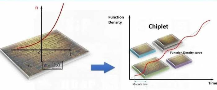
The high R&D costs and production costs cannot be sustained in proportion to the performance improvement of chips. To address this issue, the heterogeneous integration technology of chips in the "post-Moore era"—Chiplet has emerged, which may continue the "economic benefits" of Moore's Law from another dimension.
Chiplet, also known as "core grains" or "small chips," is a process that decomposes a complex SoC chip into different functional units at the design stage. Each unit is then manufactured using the most suitable process technology, and the advanced packaging technology interconnects each unit, packaging them into an SoC chip like "Lego blocks."
Advertisement
The advantages of Chiplet can be summarized in several aspects:
1) Significantly improving the yield of large chips. In recent years, with the computing demands of high-performance computing and AI, integrating more functional units and larger on-chip storage has led to a dramatic increase in the number of transistors and chip area. The chip yield decreases as the chip area increases. Designs with a mask size of 700mm² typically produce about 30% qualified chips, while the yield of 150mm² chips is about 80%. Therefore, dividing a large chip into smaller chips through Chiplet design can effectively improve the yield and reduce the cost increase caused by poor yield.
2) Reducing design complexity and design costs. If a large-scale SoC is decomposed into individual Chiplets according to different functional modules during the chip design stage, some Chiplets can achieve modular design and can be reused in different chip products. This not only greatly reduces the difficulty and cost of chip design but also facilitates subsequent product iterations and accelerates the product launch cycle.
3) Reducing chip manufacturing costs. A SoC contains different computing units, as well as storage, various I/O interfaces, analog or mixed-signal components. Among them, the logical computing units mainly rely on advanced processes to improve performance, while other parts do not have high requirements for process technology. Some can perform well even with mature processes. Therefore, after SoC is Chipletized, different core grains can be manufactured separately according to needs and then assembled using advanced packaging technology, without the need for all to be manufactured on a single wafer using advanced processes. This can greatly reduce the manufacturing cost of chips.
In short, Chiplet aims to decouple chip performance from chip processes, thereby solving the problem of a significant increase in complexity in chip design and the high cost and low yield issues faced in advanced processes.
Driven by various advantages and market trends, chip giants such as AMD, TSMC, Intel, and Nvidia, as well as many domestic and foreign related companies, have sensed market opportunities and have started to enter the Chiplet field in recent years.In this process, interconnectivity has become one of the decisive factors for Chiplet development.
Current Status of Chiplet Interconnectivity
For many years, the industry has been searching for a "true interconnect" to enable communication from die to die within a chip set, in order to better accomplish a variety of functions such as data storage, signal processing, and data handling. How to achieve high-speed interconnectivity between chiplets is key to the implementation of Chiplet technology and also a major new challenge faced by the entire industry chain.
When designing the interconnect interfaces between chiplets, chip design companies first ensure high data throughput. In addition, data latency and error rate are also key requirements, and energy efficiency and connection distance must be considered.
So far, there are more than a dozen successfully commercialized Die-to-Die interconnect interface protocols, mainly divided into serial interface protocols and parallel interface protocols. Serial interfaces and protocols include LR, MR, VSR, XSR, USR, and other SerDes serial interconnection technologies, PCIe, NVLink, CXL, CCIX, TileLink, OpenCAPI for cache coherence, and the ACC interface standard introduced by the China Chiplet Industry Alliance (CCLL); parallel interfaces and protocols include AIB/MDIO (Intel), LIPINCON (TSMC), Infinity Fabric (AMD), OpenHBI (Xilinx), BoW (OCP ODSA), INNOLINK (Innosilicon), and the HBM interface for stacked interconnection of storage chips, etc...
Comparatively speaking, serial interfaces generally have larger delays, while parallel interfaces can achieve lower delays but will consume more Die-to-Die interconnect pins. Moreover, because it is necessary to ensure the consistency of delays between multiple sets of pins as much as possible, each pin is not easy to achieve high speed.
It can be seen that these chip giants are actively exploring Chiplet technology, but at the same time, everyone is fighting their own battles, promoting their own high-speed interconnect protocol standards.
The comparison of some existing interconnect standards on the market is as follows:
Some opinions point out that there is no unified communication interface between chips of different processes, functions, and packaging, which will cause serious waste of resources.In response to this, Ma Kai, Assistant Professor at the Institute for Interdisciplinary Information Sciences, Tsinghua University, and founder of Arctic Zhongxin, said to the author that in different application scenarios, the combination form of Chiplets may be diverse. For example, the form and characteristics of data that need to be transmitted, the tolerance for delay/miscode and other indicators, the requirements for packaging, and the considerations for mass production costs may all be different. Therefore, the Die to Die interface, as a "bridge" for data transfer between chips, may also have different optimization directions in different application scenarios.
He pointed out that the so-called "going it alone" in the industry actually reflects the differentiated needs of interconnection in different product scenarios more essentially. For example, Apple's self-developed Ultrafusion solution on M1/M2 Ultra, NVIDIA's NVLink solution, and so on, are all the results of in-depth research and development by chip manufacturers and packaging manufacturers, but they are also primarily aimed at meeting their own product performance needs. Different interconnection standards differ in signal mode, transmission rate and bandwidth, packaging specifications, etc., and all reflect the direction of optimization in specific fields.
Among many interconnection standards, Intel's universal Chiplet interconnection standard UCIe has become a focus of attention in the industry.
In this regard, the author has introduced in the previous article "Chiplet, an important step forward!": UCIe aims to establish a unified standard for interconnection and intercommunication at the chip packaging level, to help build an open small chip ecosystem in the entire semiconductor industry.
UCIe is a layered protocol that specifies the physical layer, die-to-die adaptation layer, and protocol layer:
The introduction of the UCIe standard aims to help Chiplets move from "empty talk" to "practical operation", from "each family talking on their own" to "team fighting". It is hoped that the giants will work together to build a unified Chiplet interconnection standard, allowing end users to freely match small chips from multiple manufacturers' ecosystems when building SoC chips, and to accelerate the development of an open Chiplet platform.
However, looking at the current actual progress, the common point of almost all Chiplet-based designs is that they are all completed within a single company. This is far from the ideal situation where everyone hopes to pick the small chips they want from the shelves of the small chip store (Chiplet store), and then work through SiP packaging.
From the current state of the industry, whether it is UCIe or other interconnection schemes, it seems that they have not been able to take on the role of "bridge" for Chiplet interconnection interface standardization, and the dream of the small chip store is still far away.
Arctic Zhongxin also said in an interview with the author that the current significance of the introduction of the UCIe standard lies in two aspects: one is the entry of many first-line companies, which promotes the direction of technological routes in the post-Moore era; the second is to provide a feasible solution for many chip design manufacturers in the Chiplet architecture. The initial effect of assistance is obvious, and we have seen some companies start to invest in research and development from different dimensions such as UCIe interface IP, packaging solutions, but the maturity of the industrial ecosystem needs to go through an indispensable cycle of iteration.At the same time, due to the limitations of UCIe, which relies on advanced processes and has large interconnect distance constraints, UCIe can have a certain degree of uniformity within a small circle and limited scenarios, but it is difficult to apply directly to the entire Chiplet ecosystem.
Kai Sheng Ma pointed out that, looking at the current situation, there is very little work being carried out around UCIe in the industry, and it is basically still in a state of "fighting alone". On the one hand, there are no mature IPs available at present, and even if there are, they are only some overseas IP manufacturers with 5nm and 3nm ready-made IPs; on the other hand, there are not many companies doing Chiplet, even Intel's own server chip Sapphire Rapids, which is an internal closed-source port, and the silicon photonic interconnect chip demonstrated at Hot Chips this year, which is based on their more mature AIB solution.
It can be seen that, no matter what standard it is based on, the next step we need to see is the gradual introduction of available interface schemes, and more and more chip design companies using these interfaces under the standards, in order to truly form an industry interconnection standard.
The key to Chiplet technology is not only interconnection but also packaging.
As the development of Chiplet technology will ultimately lead to higher density interconnections between small chips, it is necessary to cope with the continuous improvement of advanced packaging functions and density, and heat dissipation, stress, and signal transmission are all major challenges. At present, top IDM manufacturers, wafer foundries, and packaging and testing companies are actively promoting different types of advanced packaging technologies to seize this market.
In the case of increasing chip size and complex architecture, the packaging structure has evolved from two-dimensional to three-dimensional. According to the packaging medium material and packaging process, the implementation methods of Chiplet mainly include the following: MCM, 2.5D packaging, 3D packaging. At present, TSMC has CoWoS/InFO, Intel has EMIB, Foveros 3D, etc., and the advanced packaging used by Chiplet is diverse, and new packaging forms and structures are still evolving.
However, in the field of high-performance, short-distance interconnection, interconnection generally needs to be carried out through Interposer (intermediate layer) or Silicon Bridge (silicon bridge), and the packaging cost is relatively high.
For example, the high wiring density in chip-to-chip interconnection may require the use of substrates or bridging technologies that support high wiring density. The enablement of high-bandwidth memory (HBM) may be the best proof of this trend - because HBM can only be integrated with ASICs in the same package, and at this time, it can only be integrated in a 2.5D silicon intermediate layer configuration.
Although silicon-based packaging technologies have developed into mass manufacturing solutions, cost and complexity may prevent them from becoming solutions for most low-end applications.
Chiplet interconnection technology, ushering in new breakthroughsSo far, the industry-leading interconnects for small chips require advanced packaging and costly silicon interposers.
Eliyan, with its Nulink technology, can provide an advantageous solution in terms of power consumption, performance, and cost for die-to-die interconnects on various packaging substrates. This is because this PHY interface allows different chips to achieve high-speed interconnection directly on an organic substrate without the need for costly advanced packaging methods such as CoWoS, EMIB, or silicon interposers, which reduces costs while accelerating the product manufacturing cycle.
On the left is the common Chiplet interconnection method using a silicon interposer today; on the right is Eliyan's NuLink technology, which can achieve small chip interconnection with outstanding bandwidth without the need for a silicon interposer.
It can be seen that NuLink reduces system costs by simplifying system design. More importantly, Eliyan can increase the distance between chips, and for generative AI, NuLink provides more HBM memory for each ASIC, thereby improving the performance of memory-intensive applications of GPUs and ASICs equipped with HBM.
Eliyan recently also demonstrated its first working chip of the NuLink PHY, which is implemented using a 5nm standard manufacturing process, allowing Chiplets to be mixed and matched with chips of different processes without the need for advanced packaging technologies such as silicon interposers.
NuGear eliminates the need for large silicon interposers.
This chip complies with the existing UCIe specification and can exceed the scope of the current specification, operating at a speed of 40Gbps, providing more than 2.2Tbps/mm of bandwidth at a pitch of 130um on standard organic packaging, while meeting strict power consumption and area requirements. The high-area-efficiency NuLink PHY is limited by the bump pitch, and once implemented on available standard packaging technologies with a finer bump pitch, it can provide a transmission speed of up to 3Tbps/mm by utilizing its innovative interference cancellation technology.Eliyan CEO Farjadrad pointed out: "One of the major demands in the industry today is the ability to obtain a sufficiently large interposer layer, which allows for the construction of increasingly larger GPUs or TPUs, along with large memory capacities."
Industry insiders have indicated that the maximum size of a silicon interposer is approximately 3300mm². Considering the size limitations of processing technology, currently, each SoC can only utilize six HBM3 blocks. In contrast, Nulink's organic substrate can reach three to four times the original size while providing the same or better power efficiency and bandwidth. This results in lower costs, faster manufacturing speeds, and stronger computational capabilities per package.
For example, NVIDIA can offer A100 GPUs with 40GB and 80GB HBM in two models, demonstrating that larger memory can provide a threefold performance advantage. By leveraging NuLink, the number of HBMs can be doubled to 160GB. Assuming a linear extension of memory advantages in AI training, the performance using NuLink would be increased by another threefold.
At the same time, NuLink also provides excellent thermal performance for HBM DRAM, eliminating thermal crosstalk between HBM-ASIC, allowing for a 20% increase in ASIC clock speed, as well as simpler and lower-cost cooling.
In summary, Eliyan has eliminated the need for advanced packaging, such as the limited size of silicon interposers in chiplet design, low yield, high cost, difficulty in cooling, and limited supply chain, among all related restrictions and complexities. NuLink technology can achieve DRAM expansion, material cost savings, increased yield, and shortened time to market for chips.
Eliyan believes that its chiplet interconnect product can surpass the advanced packaging technology of chip giants such as Intel and TSMC, or it may become the best choice for Intel and TSMC, thus achieving the next wave of high-performance chip architecture. Companies like NVIDIA, Intel, AMD, and Google can license NuLink IP or purchase NuGear chiplets from Eliyan to eliminate performance bottlenecks caused by silicon interposer size limitations, enabling them to achieve higher-performance AI and HPC SoCs.
Currently, Eliyan has raised $40 million in Series A funding from investors such as Intel Capital and Micron Capital to develop and improve the yield of NuLink chip-to-chip interconnect technology.
Arctic Silicon acknowledges the innovative technology of Eliyan, stating that from a macro trend perspective, this technology is one of the most intuitive and correct directions. Since bandwidth = number of wires × wire speed, when the wire speed is high, the demand for interconnect wire density can be reduced, thus allowing a transition from 2.5D packaging requirements to 2D. The D2D interconnect of Arctic Silicon also starts from this point.
However, Ma Kai also emphasized: "There are still additional considerations for Eliyan's solution. The traditional HBM approach is as follows: based on the HBM PHY, and then interconnected with the HBM Stack on the Interposer, with the specific interconnection location at a Base Die at the bottom of the HBM Stack, which has the HBM PHY interconnected with the PHY of the SoC chip. Due to the interconnection of up to 1024 wires, the Interposer 2.5D packaging was adopted when the HBM solution was born to provide an interconnect density of 40μm. When using 2D packaging, it is inevitable to increase the wire speed to exchange for a lower demand for wire density. However, the increase in speed will introduce significant additional latency and power consumption to the PHY design."Therefore, Eliyan's plan maintains the performance of bandwidth but sacrifices the advantages of low latency and low power consumption of HBM. In addition, this approach requires redesigning the Base Die of HBM, which also poses challenges for the promotion of the plan.
Overall, no matter which interconnect technology is used, each has its strengths and weaknesses and needs to be designed and selected according to actual needs. Because in the field of practical application, the characteristics of data transmission in different scenarios bring about significant differences in the demand for the adopted interface technology and packaging technology. For example:
In general computing scenarios such as CPUs, data transmission has characteristics such as high randomness, large differences in data stream structure, and high requirements for cache consistency. Therefore, in CPU Chiplet integration, great importance is often attached to optimizing indicators such as latency, and parallel transmission schemes are adopted, with a large-scale wiring that is highly dependent on the support of advanced packaging technology.
In general parallel computing scenarios such as GPGPUs aimed at the server field, data transmission has characteristics such as large volume per time, high predictability of data stream structure, and the ability to pre-load in advance. Therefore, in Chiplet integration, it is necessary to focus on optimizing indicators such as bandwidth and can adopt parallel or serial schemes, with a high dependence on advanced packaging.
In specific AI acceleration scenarios, it is necessary to comprehensively consider the cost sensitivity, operating environment, and other requirements, and adopt different interface technologies and packaging solutions to meet the differentiated needs of end users: for example, in the field of intelligent driving, advanced packaging solutions often do not meet vehicle specifications, and the mass production cost is also high. When using Chiplet heterogeneous integration, it is often necessary to consider optimizing the corresponding D2D technology on the basis of mature packaging solutions.
Ma Kaisheng emphasized that Chiplet interconnect technology should be continuously iterated and upgraded based on scene requirements and the maturity of the supply chain, and it is not necessarily pursuing a unified standard. In the process of Chiplet development, different companies in the industry will participate from the perspectives of chiplet design, standard development, and packaging technology, and ultimately need to truly solve the pain points of downstream businesses while taking into account performance, cost, and other factors, and naturally become industry standards.
In this process, it has also brought new development opportunities for domestic enterprises, and manufacturers have also taken action in recent years.
For example: Xin Dong Technology has launched domestic independent standard INNOLINK Chiplet IP and HBM2E and other high-performance computing platform technologies, supporting high-performance CPU/GPUINPU chips and servers; in order to make IP more concrete and flexible in Chiplet, Xin Yuan has proposed the concept of IP as a Chip (laaC), aiming to achieve special function IP from soft to hard "plug and play" in Chiplet, reducing the design time and risk of large-scale chips.
In addition, as early as 2020, the Arctic Bear Chip launched the "China Chiplet Industry Alliance" with domestic upstream and downstream, and the alliance launched the "Chiplet Interconnect Interface Standard" based on the optimization of the domestic packaging supply chain at the beginning of 2023, aiming to provide high-performance, low-cost interconnection solutions for high-performance heterogeneous integrated chips such as GPUs, AI, and large SoCs. Currently, the first interface has been successfully tested back to the chip.On how domestic enterprises should better participate in the Chiplet industry ecosystem, Arctic Core believes that domestic enterprises should be based on the large domestic market demand, and focus on a Chiplet commercial landing model of "independent and controllable" supply chain, which is more in line with the realistic and objective environment. The industry's upstream and downstream should jointly promote the establishment of the domestic Chiplet industry ecosystem, and in this chain, the role of Chiplet chip design companies is extremely important. Design companies are closest to the needs of downstream customers, and can comprehensively consider the performance, power consumption, cost sensitivity and other factors of downstream scenarios, accurately define various "core grain" products, and in turn, jointly promote the iterative upgrade of the supply chain with upstream IP manufacturers, wafer manufacturers, packaging manufacturers, and substrate manufacturers, to achieve an "independent and controllable" domestic Chiplet industry ecosystem, which is more realistic and meaningful.
Conclusion
According to Gartner data statistics, the sales revenue of semiconductor devices based on Chiplet was only 3.3 billion US dollars in 2020, and has exceeded 10 billion US dollars in 2022. It is expected to exceed 25 billion US dollars in 2023 and reach 50.5 billion US dollars in 2024, with a compound annual growth rate of 98%, and the market space is huge.
The heterogeneous integrated chip technology based on Chiplet represents the research and development direction of complex chip design in the "post-Moore era". Chiplet, a technology that decouples chip performance from the process, has opened up a new development path for the development of integrated circuit technology.
However, as an emerging technology, Chiplet is currently in the development stage. Whether it can become a new IP product and business model, or even the savior of Moore's Law, the key lies in whether the industry can reach a unified Chiplet interconnection standard and establish an open and standardized Chiplet ecosystem.
In this process, Chinese Chiplet academia and industry should seize the opportunity, increase investment in technology research and development and standard setting, and master core technologies as soon as possible. In addition, chip industry participants need to avoid going it alone and should focus on ecosystem construction, and establish an industry-accepted standard for heterogeneous integrated technology based on Chiplet as soon as possible, in order to occupy a place in future international competition.
Leave A Comment