Apple, playing with advanced packaging.
On November 21, 2017, Zhang Zhongmou, then chairman of TSMC, was quietly clapping in the audience. The protagonist of this day was not the famous him, but Yu Zhenhua, who was previously unknown.
After receiving the award, he pointed to the iPhone in the hands of a reporter on the side and said: "This has InFO (Integrated Fan-Out Packaging), which started from the iPhone 7 and is still being used now, the iPhone 8, the iPhone X, and other mobile phones will start using this technology in the future."
The InFO mentioned here is a type of advanced packaging, which made TSMC easily take all the orders of the A10 processor in the iPhone 7, and squeezed out Samsung, which was still processing the A9 processor in 2015, and established the position of TSMC.
Relying on InFO, the Apple A10 processor still achieved a good performance improvement while using the 16nm FinFET process, and it was not much inferior to the Snapdragon 835 and Exynos 8890 using Samsung's 10nm process.
At this time, the sharp weapon of advanced packaging, through the hands of Apple, unveiled its mysterious veil and came to the world.
Advertisement
Packaging, feeling the stones across the river
The story of Apple and advanced packaging may have to start from 2007.
Nokia N95 - a smartphone released in March 2007, its motherboard not only has a powerful dual processor, but also a dense analog chip, and its complexity is not less than any high-end notebook at that time.
At the same time, the N95 also has three different storage chips, scattered around the two processors, just to understand the hardware architecture of this phone, it takes a lot of effort, and it is also a very troublesome thing to repair.
And another motherboard picture also comes from the mobile phone released in 2007 - the first generation of the iPhone, after careful observation, we will find that the integration of the entire motherboard is higher than the N95, and various chips are densely arranged together, and the gap between each other is greatly shortened.More importantly, on this motherboard, we can only find the processor and NAND, but the DRAM that can be seen in all mobile phones has disappeared. Does Apple have any black technology that can put DRAM on the auxiliary board?
The answer is hidden under the Apple logo chip. This SoC, named APL0098, is actually a rebranded version of Samsung's S5L8900. Underneath it, two 512 MB SDRAMs from Samsung are stacked and packaged. Yes, that's right, Apple used stacked packaging (PoP) on the first-generation iPhone, integrating DRAM and SoC together.
This technology, of course, also comes from Samsung. At that time, TSMC also had to admit defeat. From the first-generation iPhone to the iPhone 5s, all Apple processors and packaging were completed by Samsung alone. Even the development of Apple's A4 self-developed chip was greatly influenced by Samsung.
A semiconductor person from Taiwan, China, commented that Samsung is the only semiconductor factory in the world that can mass-produce storage and processors and has its own packaging and testing factory. It is manufactured by it, and the entire A7 processor can be completed under "one roof", with huge advantages in cost and integration. TSMC is indeed difficult to catch up in a short period of time.
There is no reason for Apple to favor PoP packaging. Compared with traditional packaging, PoP packaging occupies less substrate, and the smaller size and lighter weight in turn reduce the circuit board area. The shorter interconnection with DRAM can achieve faster data transmission rates, and costs can be saved at every stage of the manufacturing process.
The advanced packaging on the iPhone 5s is just a small trial for Apple. Apple really used this sharp weapon well, and it had to wait until the Apple Watch in 2014.
At the September launch of this year, Apple's CEO Cook prepared "One More Thing" again after many years, but this time the protagonist was the smart wearable. After the iPad, Apple launched the Apple Watch, a new category.
At the launch, Cook also praised it a lot. Although the Apple Watch is not the earliest smart watch on the market, Cook still regards it as a revolutionary product. "It is not a mini version of the iPhone, but an innovative way of communication 'directly through the wrist', and its functions are far more than these." Cook said on the stage.
Many advanced functions of the Apple Watch are now very common, and most smart watches at the level of one thousand yuan can easily do it, but its core - the S1 chip is something other manufacturers have never caught up with.
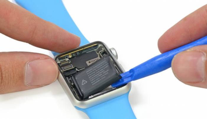
When the disassembly organization lifted the screen of the Apple Watch, only a battery and a linear vibration motor could be seen, and the processor driving the watch was gone. Until the battery was lifted, the packaged chip with the Apple logo was finally revealed.The chip imprinted with S1 is firmly pressed under the battery and motor, and the packaging technology it uses is exactly the SiP (System in a Package system-level packaging) that we are talking about today.
Disassembly shows that SiP packaging truly reflects the essence of packaging the entire system. On a motherboard with a size of 26.15 mm x 28.50 mm, it integrates as many as 14 core chip products, as well as hundreds of resistors, capacitors, and other components. All components have their own independent packaging and are closely and orderly arranged on the motherboard. Except for the inertial combination sensor, other components are all packaged together, and the entire packaging thickness is only 1.16mm.
26.15 mm x 28.50 mm x 1.16mm, the size of traditional chips, constitutes a system, and its complexity even surpasses the iPhone 6 motherboard that was released with it at that time.
However, behind the advanced packaging, it is no longer the familiar Samsung that is in charge. Apple has turned its attention to Taiwan, China. Although wafer foundry is a well-known advantage here, TSMC is responsible for the foundry of the A8 chip. However, as a very important part of semiconductors, packaging and testing are not much inferior to other countries and regions.
Who is behind the S1 chip? According to media reports, the SiP substrate of S1 comes from King Yuan Electronics and Nan Ya, while the SiP packaging and module foundry are monopolized by the packaging and testing giant ASE. The three major suppliers have come together for Apple, injecting a powerful power into the small body of the first-generation Apple Watch.
PoP plus SiP, Apple groped its way over the river, stepping out its own path in advanced packaging.
Strong alliance, change the world
Seeing that advanced packaging has become more and more popular since the first-generation iPhone, Apple has also started to consider more advanced packaging forms. Samsung's PoP alone is no longer enough for Apple, and thinner packaging has become a necessity.
TSMC, which has processed A8 and some A9 chips, has introduced a technology that Apple cannot refuse - InFO.
In fact, TSMC has been laying out packaging since 2009, with the leader being Morris Chang, and the developer is Yu Zhenhua, who created the CoWoS that is currently popular in AI.At that time, Zhang Zhongmou was extremely optimistic about the direction of advanced packaging and even allocated 400 R&D engineers to Yu Zhenhua. He lived up to expectations and successfully developed the first generation of CoWoS technology three years later.
This technology, released in 2011, was first adopted by Xilinx's high-end FPGAs. The largest size of the Si interposer layer is 775mm² (25 mm x 31 mm), close to the exposure size of a reticle (26mm x 33mm) under ArF immersion lithography, while the FPGA chip manufacturing technology is 28-nanometer CMOS process. The high-end Xilinx FPGA "7V2000T" using this technology is equipped with four FPGA logic chips in "CoWoS_S".
In the second generation "CoWoS_S" released in 2014, the silicon interposer layer was expanded to 1150mm², close to 1287mm², which is the exposure area of a 1.5-division plate. It was adopted by Xilinx's high-end FPGA "XCVU440" in 2015, which uses a 20-nanometer CMOS process and is equipped with three FPGA logic chips.
The two consecutive generations of CoWoS did not cause much of a stir, and only Xilinx became a customer of TSMC's new technology, which also made Yu Zhenhua, who developed the technology, waver. "(It seems that) someone made a big promise, took a lot of resources, and made something that didn't seem very useful," he recalled in a subsequent interview.
Is the CoWoS technology not good enough? Of course not. In theory, processors using this technology can reduce the thickness by up to 70%. For the precious semiconductor industry, this temptation is not small.
However, what discouraged them was the cost of CoWoS. Some TSMC customers indicated during negotiations that such technology would be accepted only if the price did not exceed 1 cent per square millimeter, but the price of CoWoS reached more than 5 times that, and even large companies would inevitably feel the pain.
In order to change the situation of being well-received but not popular, the senior management of TSMC decided to develop an advanced packaging technology at 1 cent per square millimeter, with slightly lower performance than CoWoS, but it must strive to attract major customers.
This technology was first used in the InFO packaging of iPhone 7 and 7Plus, and ultimately became the key to TSMC's complete order of Apple's A10 chip.
InFO stands for Integrated Fan-Out, which means integrated fan-out packaging, focusing on integration and fan-out packaging. When mentioning InFO packaging, we first need to talk about FOWLP (Fan-Out Wafer Level package) packaging. Traditional WLP packages before cutting, although reducing the packaging size, but limiting the number of I/O, in order to meet the increasing demand for I/O, FOWLP came into being. FOWLP uses fan-out technology, through the RDL layer, expands the contact points on the surface of the Die to beyond the projected area of the Die, increasing the flexibility of the arrangement of bumps and increasing the number of pins. The characteristics of the general FOWLP package are small size, no substrate, and plastic encapsulation. InFO packaging has the same characteristics as FOWLP in some aspects, but also develops on it.
Generally speaking, InFO packaging includes three types: InFO_oS, InFO_PoP, and InFO_LSI. What TSMC provides to Apple is InFO_PoP packaging, whose full name is Integrated Fan-out Package on Package, which is a combination of FOWLP and PoP packaging. It stacks different types of chips vertically, with the lower layer being the chip packaged in FOWLP, and the upper layer being DRAM and other passive chips, with electrical interconnection between the packages through TIV (Through Info Via).Compared to the PoP packaging provided by Samsung, InFO_PoP does not require a silicon interposer, allowing multiple flip-chip components to be placed on the packaging substrate and interconnected through the packaging substrate, not only reducing the chip area and thickness but also being more competitive in price.
According to a senior executive of a packaging and testing factory who has been involved in Apple's orders, Samsung was somewhat careless. When TSMC proposed InFO, Samsung, with more packaging experience, thought that as long as the existing PoP packaging was slightly improved, it could meet the thickness requirements of Apple, but the facts obviously proved otherwise.
The InFO technology has been improved several times and is not only used in the iPhone to this day but also benefits the Mac products.
When Apple launched the 20-core M1 Ultra processor in 2021, its UltraFusion 2.5 TB/s processor interconnection attracted global attention, and how to achieve this has become a concern for all semiconductor industry insiders.
Behind it is the iterative version of Info_PoP - Info_LSI technology.
Info_LSI packaging, full name Integrated Fan-out_Local Silicon Interconnect, uses silicon bridges and RDL layers instead of a whole piece of silicon to achieve a balance between performance and cost. According to TechInsights' analysis, the silicon bridge connects two M1 Max processors together, achieving low resistance, low latency, and high bandwidth. The M1 Ultra is also the first device example recorded by TechInsights to use InFO-LSI technology.
Advanced packaging not only firmly bonds the two processors together but also builds a silicon bridge between Apple and TSMC. The two giants join hands to set off a storm about packaging.
The next advanced packaging chip
For Apple, it seems completely impossible to be satisfied with the existing packaging technology. Even TSMC, which is far ahead in the process, has been at the 5nm node for a long time until it completed the large-scale mass production of the 3nm node this year. As for the more distant GAA and 2nm, it is definitely difficult to achieve quickly in the short term.As a company that started out as an electronic consumer product company, Apple has a kind of obsession with performance that is beyond ordinary companies. The performance of the processor in the mobile phone must be iterated every year. The new self-developed chip version of Mac needs to maintain its leading performance and power consumption under the pressure of Intel and AMD. Today, as Moore's Law gradually fails, TSMC's advanced packaging has become Apple's magic weapon. According to Taiwanese media reports, Apple is trial-producing the latest 3D chip stacking technology SoIC (single-line integrated circuit small outline package) in small quantities. It is currently planning to use SoIC with InFO packaging solutions, which are expected to be used in MacBooks and will be launched as early as 2025~2026. What is the new technology of SoIC? According to TSMC's explanation at the 24th Annual Technology Seminar, SoIC is an innovative multi-chip stacking technology, a wafer-on-wafer bonding technology, which is a 3D IC process technology that allows TSMC to have the ability to directly produce 3D ICs for customers. What is most amazing is that SoIC technology uses through silicon via (TSV) technology, which can achieve a bump-free bonding structure and integrate many adjacent chips of different properties. The most critical and mysterious part is the bonding material, which is said to be a confidential material worth up to one billion US dollars. Therefore, it can directly communicate multiple layers of chips through tiny gaps, achieving more than multiple times the performance in the same volume. In short, it can continue to maintain the advantages of Moore's Law. When TSMC went to Japan to participate in the VLSI Technology and Circuit Seminar to publish a technical paper, it also published a paper on SoIC technology, stating that the SoIC solution stacks bare chips of different sizes, process technologies and materials together. Compared with traditional three-dimensional integrated circuit solutions using micro-bumps, TSMC's SoIC has several times higher bump density and speed, while greatly reducing power consumption. In addition, SoIC can use TSMC's InFO or CoWoS back-end advanced packaging technology to integrate other chips to create a powerful 3D×3D system-level solution. Some media believe that from the CoWoS technology initially proposed by TSMC to the InFO technology that exclusively manufactures Apple, the next technology that will make it the leader in the packaging industry is the SoIC technology. Currently, TSMC's SoIC technology has entered mass production at Zhunan Plant 6 (AP6), with a monthly production capacity of nearly 2,000 pieces, and is expected to continue to double in the next few years. AMD is its first customer, and the latest MI300 uses the SoIC combined with CoWoS packaging solution. Based on cost, design and other factors, Apple is likely to adopt the SoIC combined with InFO solution, and perhaps the strength of this technology can be seen on the M3 Ultra. PoP technology led the iPhone into the smartphone market, and InFO put Apple's self-developed mobile chips on the road to rise. Will SoIC bring about a new packaging revolution for Apple's desktop chips?
Leave A Comment